
Liquid crystal display element and pixel structure

a liquid crystal display element and pixel structure technology, applied in static indicating devices, instruments, non-linear optics, etc., can solve problems such as affecting aperture rate, many defects in the design of pixels, vertical crosstalk, etc., to reduce vertical crosstalk, maintain pixel transmittance and symmetry of view angle, and high quality

Active Publication Date: 2009-05-28
AU OPTRONICS CORP
View PDF8 Cites 16 Cited by
  • Summary
  • Abstract
  • Description
  • Claims
  • Application Information

AI Technical Summary

Benefits of technology

[0010]The invention is directed to a liquid crystal display element capable of reducing vertical crosstalk of pixels and maintaining pixel transmittance and symmetry of view angle so that the manufactured element has high quality, the manufacturing process is free of metal line short-circuiting and has high yield rate due to the pixel design.

Problems solved by technology

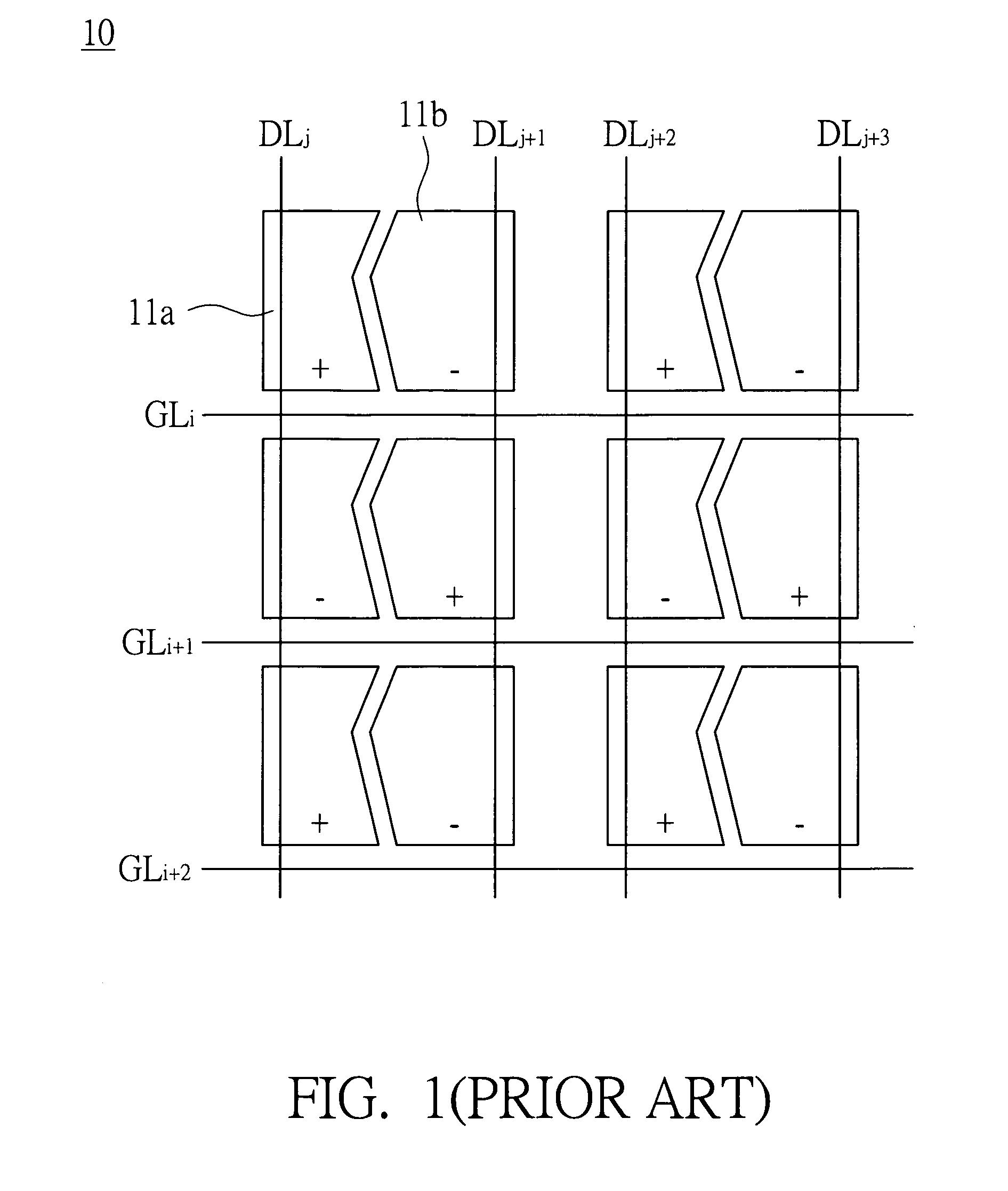
However, there are many defects in the design of pixels as indicated in FIG. 1.
Due to the capacitance coupling effect between the data lines and the transparent electrode, the pixel area that is not driven originally will be affected by the driving of neighboring pixel area and result in the problem of vertical crosstalk.
Moreover, the design of disposing the data lines within the transmitting area will affect the aperture rate and decrease the transmittance.

Method used


Image

  • Liquid crystal display element and pixel structure
  • Liquid crystal display element and pixel structure
  • Liquid crystal display element and pixel structure

Examples


first embodiment

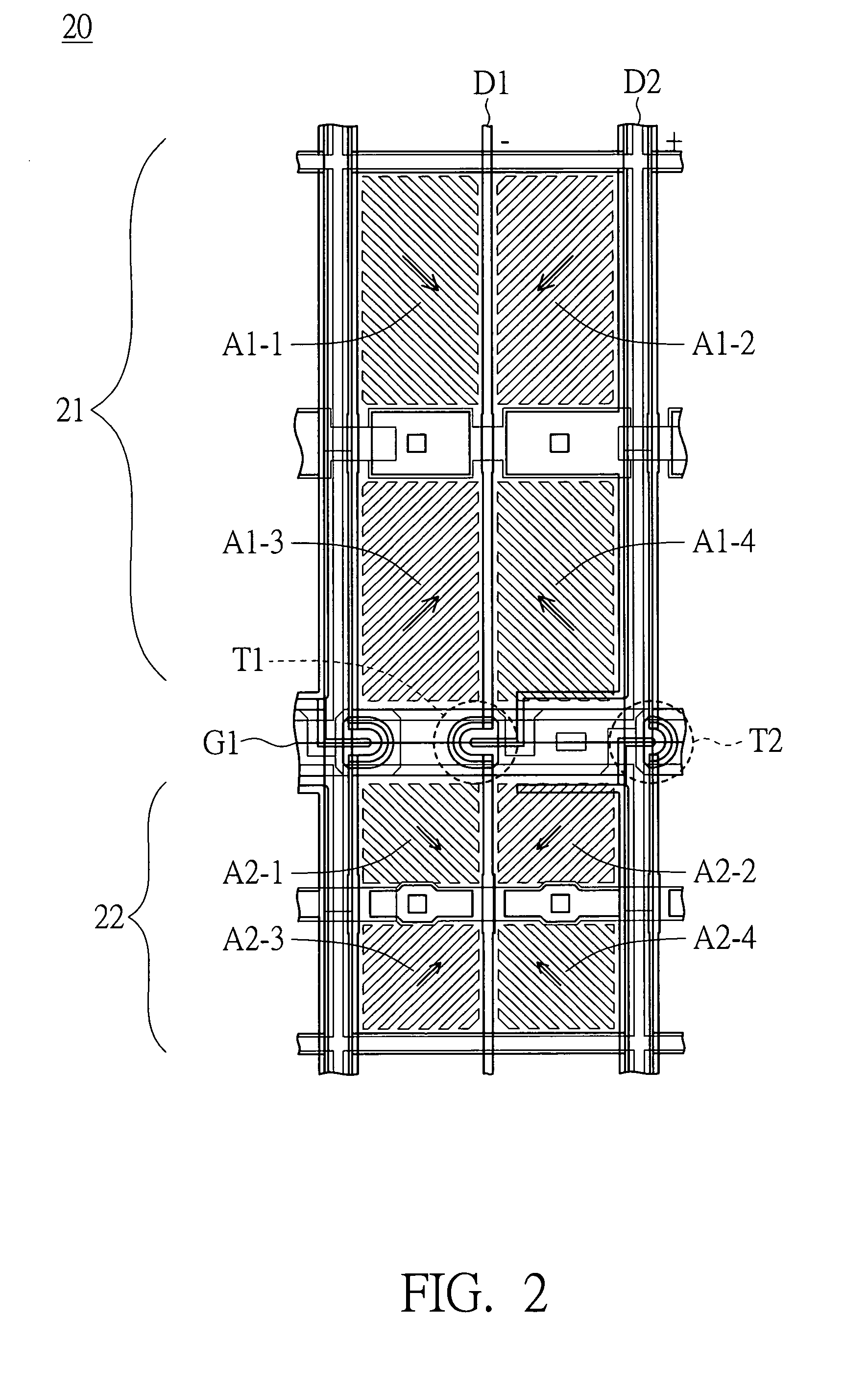
[0037]FIG. 2 is a structural diagram of a single pixel area according to a first embodiment of the present invention. As indicated in FIG. 2, the liquid crystal display element 20 includes a first data line D1, a second data line D2 and a gate line G1 substantially crisscrossed with the first data line D1 and the second data line D2. Each pixel area includes a first sub-pixel area 21 and a second sub-pixel area 22 neighboring the first sub-pixel area 21, wherein the first sub-pixel electrode and the second sub-pixel electrode are respectively disposed in the first sub-pixel area 21 and the second sub-pixel area 22. The first sub-pixel electrode in the first sub-pixel area 21 and the second sub-pixel electrode in the second sub-pixel area 22 respectively correspond to four display domains. In the present embodiment of the invention, the area of the first sub-pixel area 21 is larger than that of the second sub-pixel area 22.

[0038]The first data line D1 is disposed at the interface bet...

second embodiment

[0047]In the second embodiment, it is exemplified by taking two neighboring pixel areas as a unit for constructing a display element. To drive the display element can be viewed as to operate pixel elements in these pixel areas. The structure and the operation of a pixel element are illustrated in details as below. Noted that the second embodiment is for illustrating one of the methods of driving the pixel elements of the invention not for limiting the scope of protection of the invention.

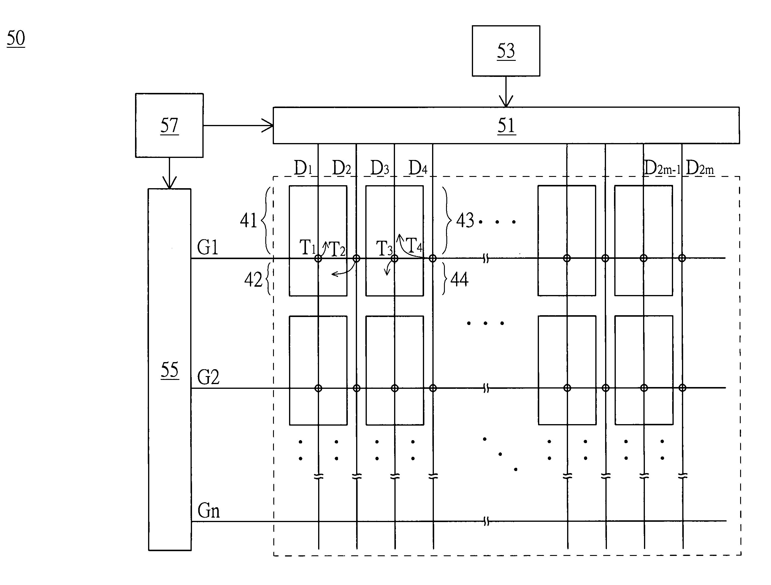
[0048]FIG. 3 is a structural diagram of two pixel areas according to a second embodiment of the present invention. The pixel elements are disposed in two neighboring pixel areas. As indicated in FIG. 3, a first pixel element and a second pixel element of the liquid crystal display element 30 are respectively disposed in a first pixel area 31 and a second pixel area 32, wherein the first pixel area 31 includes a first sub-pixel area 41 and a second sub-pixel area 42, and the second pixel area 32 incl...


PUM

PropertyMeasurementUnit
contained angleaaaaaaaaaa
contained anglesaaaaaaaaaa
areaaaaaaaaaaa

Abstract

A pixel structure of liquid crystal display including a first and a second sub-pixel electrodes, a first and a second data lines, a gate line, and a first and a second transistors is provided. The first and the second sub-pixel electrodes disposed in the first and second sub-pixel areas respectively include at least two display domains at left and right. The first data line is disposed under the interface between two domains of each of the first and second sub-pixel electrodes, and the second data line is disposed under the edges of the first and second sub-pixel electrodes. The gate line is disposed between the first and second sub-pixel areas. The first sub-pixel electrode is controlled by the gate line and the first data line through the first transistor. The second sub-pixel electrode is controlled by the gate line and the second data line through the second transistor.

Description

[0001]This application claims the benefit of Taiwan application Serial No. 96145132, filed Nov. 28, 2007, the subject matter of which is incorporated herein by reference.BACKGROUND OF THE INVENTION[0002]1. Field of the Invention[0003]The invention relates in general to a pixel structure of liquid crystal display element, and more particularly to a pixel structure of a liquid crystal display element capable of reducing vertical crosstalk effect and having high transmittance.[0004]2. Description of the Related Art[0005]Along with the rapid growth in the demand for portable products such as personal digital assistant (PDA), cellular phone, projector and large-sized projection TV, the demand for liquid crystal display (LCD) also grows, and consumers are requesting perfect display quality of the portable products. And how to improve product yield rate and make the quality meet consumers' request has become an essential factor in the design of display elements to manufacturers of LCD elem...

Claims


Application Information

Patent Timeline
Patent Type & Authority Applications(United States)
IPC IPC(8): G02F1/133G02F1/1343
CPCG02F1/133707G02F1/134336G02F1/13624G09G2320/0209G09G3/3614G09G3/3648G09G2300/0443G02F2001/134345G02F1/134345
Inventor SU, TING-WEILIAO, PEI-CHUNHOU, HUNG-LUNG
Owner AU OPTRONICS CORP
Learn More