
Electro-optical device, method of driving electro-optical device, and electronic apparatus

a technology of electrooptical devices and electrooptical devices, applied in the direction of electric digital data processing, instruments, computing, etc., can solve the problems of increasing drive voltage levels, difficult to supply correction voltage levels appropriate to the and requiring considerable time for supplying the correction voltage level to the whole plurality of data lines. , to achieve the effect of reducing vertical crosstalk and high quality images

Inactive Publication Date: 2012-03-20
SEIKO EPSON CORP
View PDF6 Cites 13 Cited by
  • Summary
  • Abstract
  • Description
  • Claims
  • Application Information

AI Technical Summary

Benefits of technology

The invention provides an electro-optical device with improved display quality by reducing vertical crosstalk and other factors that affect image quality. This is achieved by simultaneously outputting a correction voltage and sequential data voltages to multiple data lines, and distributing the correction voltage to the data lines in a way that ensures uniform voltage levels. The correction voltage is simultaneously supplied to multiple data lines, reducing power consumption and improving display quality. The correction voltage can be set without depending on the gray scale level of the pixels, and can be applied to data lines instead of individual pixels to prevent unbalanced voltages. Overall, the invention provides a high-quality display with reduced crosstalk and improved image quality.

Problems solved by technology

However, in the above-described technology for sequentially supplying the correction voltage level to a plurality of data lines, one at a time, there are technical problems that a considerable time is required for supplying the correction voltage level to the whole plurality of data lines and that a drive voltage level increases.
On the other hand, in the technology for simultaneously supplying the correction voltage level to the plurality of data lines, there is a technical problem that it is difficult to supply correction voltage levels appropriate to the plurality of data lines.
Thus, even in a case where unbalance among the data lines is generated in a period during which the data voltages are supplied after the correction voltage is supplied, the unbalance can be averaged.

Method used


Image

  • Electro-optical device, method of driving electro-optical device, and electronic apparatus
  • Electro-optical device, method of driving electro-optical device, and electronic apparatus
  • Electro-optical device, method of driving electro-optical device, and electronic apparatus

Examples


first embodiment

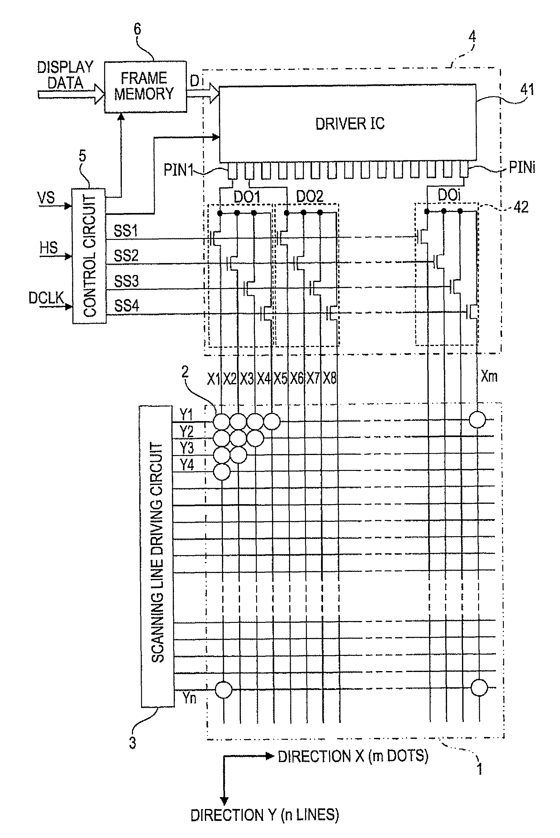
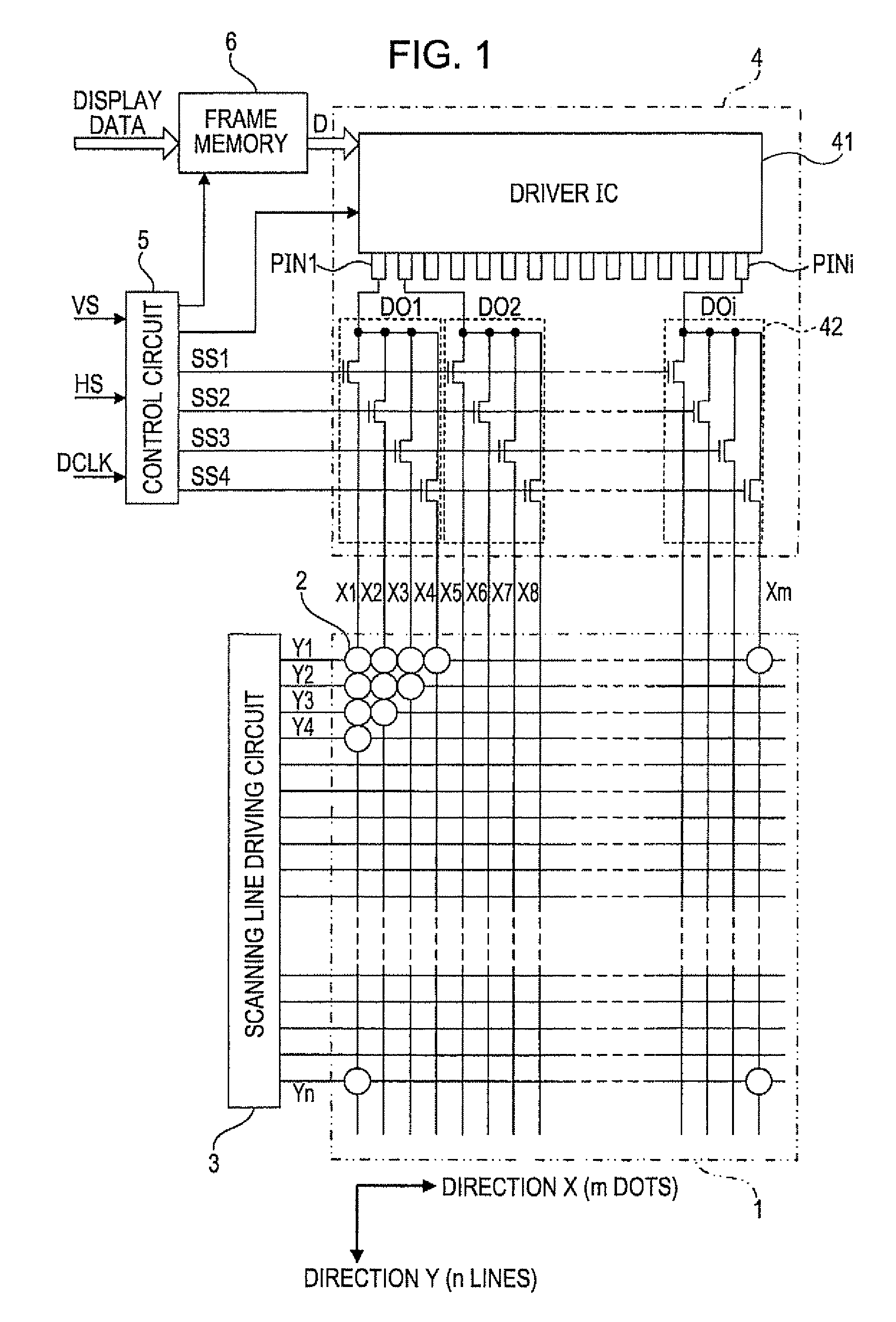
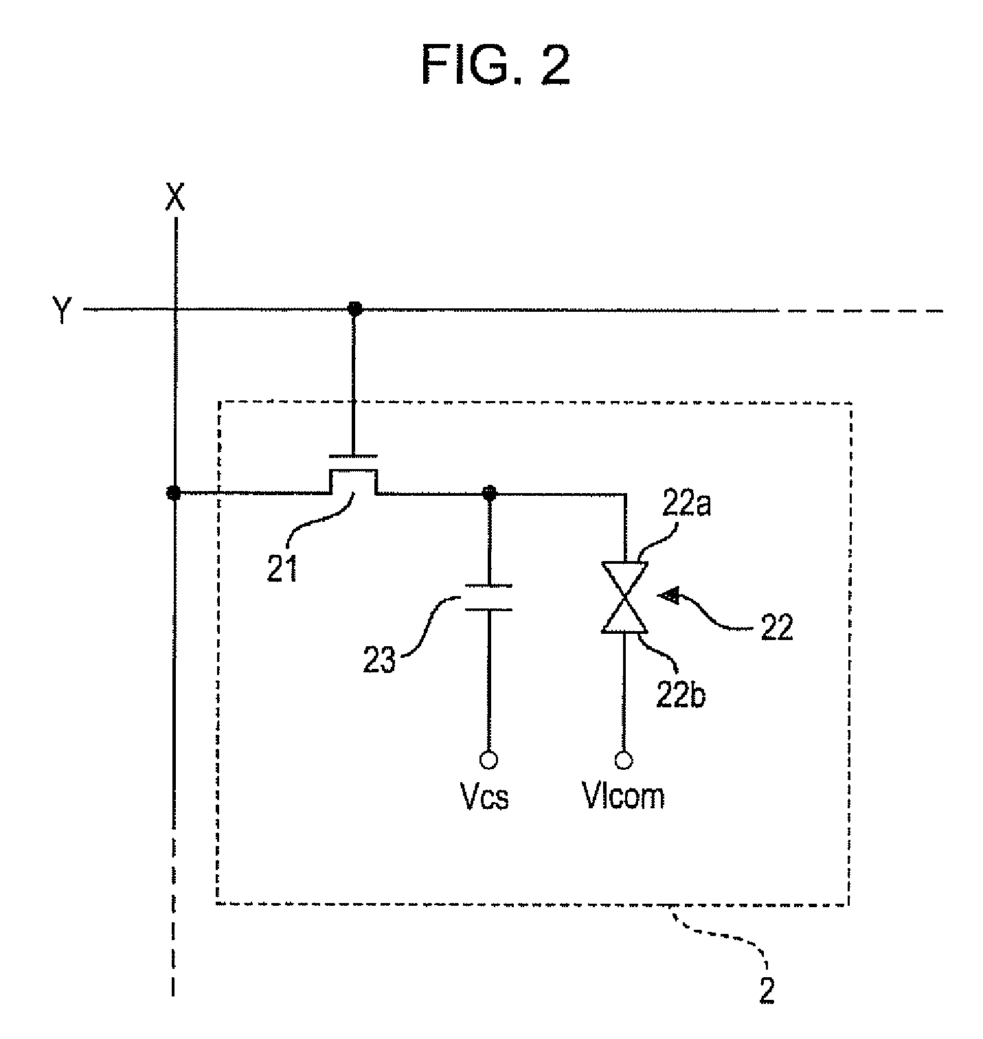
[0042]First, an electro-optical device according to a first embodiment of the invention will now be described with reference to FIGS. 1 to 4. FIG. 1 is a block diagram showing the configuration of the electro-optical device according to this embodiment. FIG. 2 is an equivalent circuit diagram showing the configuration of a pixel unit according to this embodiment. FIG. 3 is a block diagram showing the configuration of a driver IC according to this embodiment. FIG. 4 is a timing chart of a process for time division drive in an electro-optical device according to this embodiment.

[0043]In FIG. 1, a display unit 1, for example, is an active matrix type display panel that drives a liquid crystal device by using a switching element such as a TFT (Thin Film Transistor). In this display unit 1, pixels 2 corresponding to m dots×n lines are arranged in the shape of a matrix (in a two dimensional plane). In addition, in the display unit 1, N scanning lines Y1 to Yn that extend in a line directi...

second embodiment

[0068]Next, an electro-optical device according to a second embodiment of the invention will be described with reference to FIG. 5. FIG. 5 is a timing chart of a process for time division drive in an electro-optical device according to the second embodiment.

[0069]In FIG. 5, the time division circuit 42 sequentially supplies the correction voltage Vamd to the data lines X1 to X4 during a supply period T1 that is shorter than a distribution period T2 during which the sequential data voltage (for example, V1 to V4) is distributed to the data lines X1 to X4. Other features of the second embodiment are the same as those of the above-described first embodiment, and thus, a description thereof is omitted here.

[0070]According to this embodiment, by setting the correction voltage supply period T1 to be shorter than the voltage distribution period T2, the data recording period can be easily acquired (especially, the time limitation on the pixel column corresponding to the data line X4 is reli...

third embodiment

[0071]Next, an electro-optical device according to a third embodiment of the invention will be described with reference to FIG. 6. FIG. 6 is a block diagram showing the configuration of the driver IC according to the third embodiment.

[0072]As shown in FIG. 6, the configuration of the driver IC 41 has a different from that shown in FIG. 3 that the selector switch groups 41d are disposed in the rear end of the D / A converter circuit 41e. In addition, since inputs of the selector switch groups 41d are analog voltages, each selector switch group 41d is constituted by only four switches shown in the figure, which is different from the selector switch group in a case shown in FIG. 3 (that is, a configuration in which 6-bit switch groups are arranged). Other features of the third embodiment are the same as those of the first embodiment, and thus, a same reference code is attached to a same element as that in the first embodiment, and a description thereof is omitted here.

[0073]To each selec...


PUM


Abstract

An electro-optical device includes data lines divided into groups of M data lines, where N is a natural number equal to or greater than three. Output lines are arranged in correspondence with the data lines and receive, during a predetermined period, output of a correction voltage having a predetermined voltage level and sequential data voltages for defining gray scale levels of the pixels. A time division circuit simultaneously supplies the correction voltage output to the output line to M data lines of each group of data lines, where M is a natural number equal to or greater than two and equal to or less than “N−1”.

Description

BACKGROUND[0001]1. Technical Field[0002]The present invention relates to technical fields of an electro-optical device such as a liquid crystal device, a method of driving the electro-optical device, and an electronic apparatus such as a liquid crystal projector having the electro-optical device.[0003]2. Related Art[0004]In electro-optical devices of this type, parasitic capacitance exists between a data line to which a data voltage for regulating a gray scale level of a pixel is supplied and a pixel column connected to the data line. The data line and the pixel column form capacitance coupling through the parasitic capacitance, and there is a case where vertical crosstalk (uneven display in a direction along the data line) is generated due to the capacitive coupling and the like during the operation of the device. In addition, there is a case where the vertical crosstalk is generated due to a gradual variance of a voltage level maintained in a pixel which is influenced by a leakage...

Claims


Application Information

Patent Timeline
Patent Type & Authority Patents(United States)
IPC IPC(8): G09G5/00
CPCG09G3/002G09G3/3688G09G3/2011G09G2310/0218G09G2310/027G09G2360/18
Inventor ITO, AKIHIKO
Owner SEIKO EPSON CORP
Learn More