Solid-state imaging device, fabrication method thereof, imaging apparatus, and fabrication method of Anti-reflection structure

a fabrication method and imaging device technology, applied in non-linear optics, instruments, optical elements, etc., can solve the problems of difficult formation of protruding patterns according to nanoimprinting methods, sensitivity decrease, and difficulty in stably forming protruding patterns, etc., to achieve stably and easily, and form stably and easily

Inactive Publication Date: 2010-09-30
SONY CORP
View PDF11 Cites 94 Cited by
  • Summary
  • Abstract
  • Description
  • Claims
  • Application Information

AI Technical Summary

Benefits of technology

[0035]Embodiments of the present invention enable suppressing sensitivity reduction caused by formation of an anti-reflection structure, and on the contrary, enables increasing sensitivity, suppressing shading, and preventing reflections. In addition, embodiments of the present invention enable fabrication of an anti-reflection structure according to a nanoimprinting method.
[0060]In the imaging apparatus according to the embodiment of the present invention, since a solid-state imaging device capable of obtaining high-quality images with high sensitivity is used, it is possible to provide an advantage that high-quality images can be obtained with high sensitivity.

Problems solved by technology

One existing problem with the related art is that it is difficult to stably form the protrusion pattern which is suitable for an anti-reflection structure.
Another existing problem with the related art is that sensitivity decreases when the relief structure is formed exceeding a certain aspect ratio.
In addition, if the aspect ratio is too large, the formation of the protrusion pattern according to the nanoimprinting method is difficult due to the difficulties in mold separation.

Method used


Image

  • Solid-state imaging device, fabrication method thereof, imaging apparatus, and fabrication method of Anti-reflection structure
  • Solid-state imaging device, fabrication method thereof, imaging apparatus, and fabrication method of Anti-reflection structure
  • Solid-state imaging device, fabrication method thereof, imaging apparatus, and fabrication method of Anti-reflection structure

Examples


first embodiment

1. First Embodiment

Example of First Fabrication Method of Anti-Reflection Structure

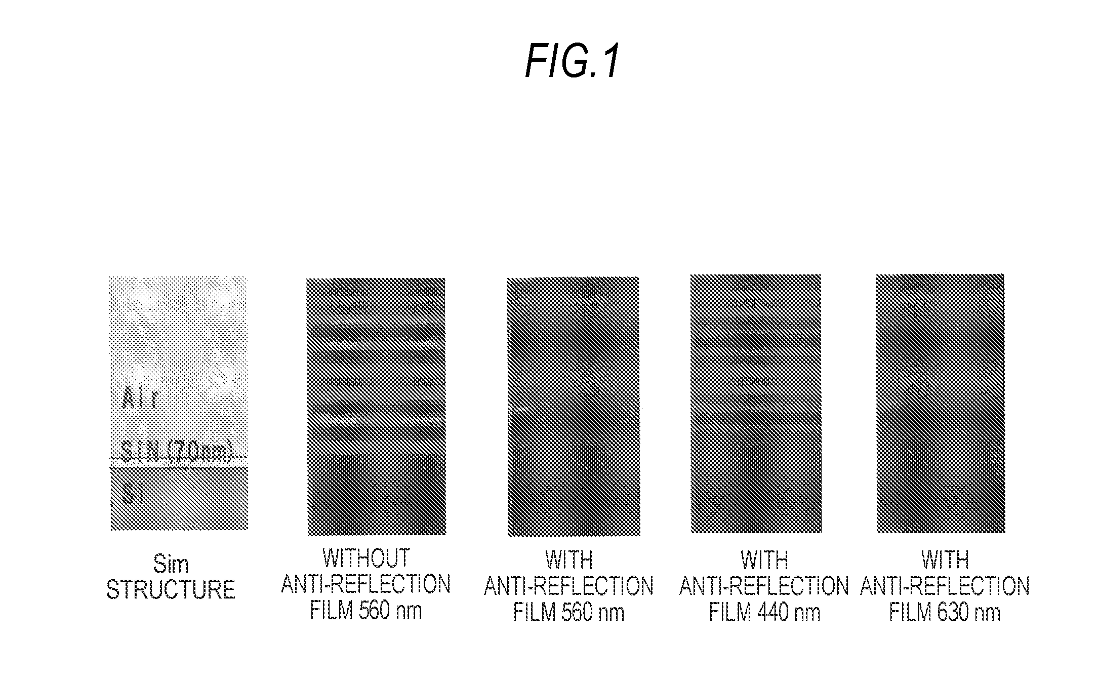
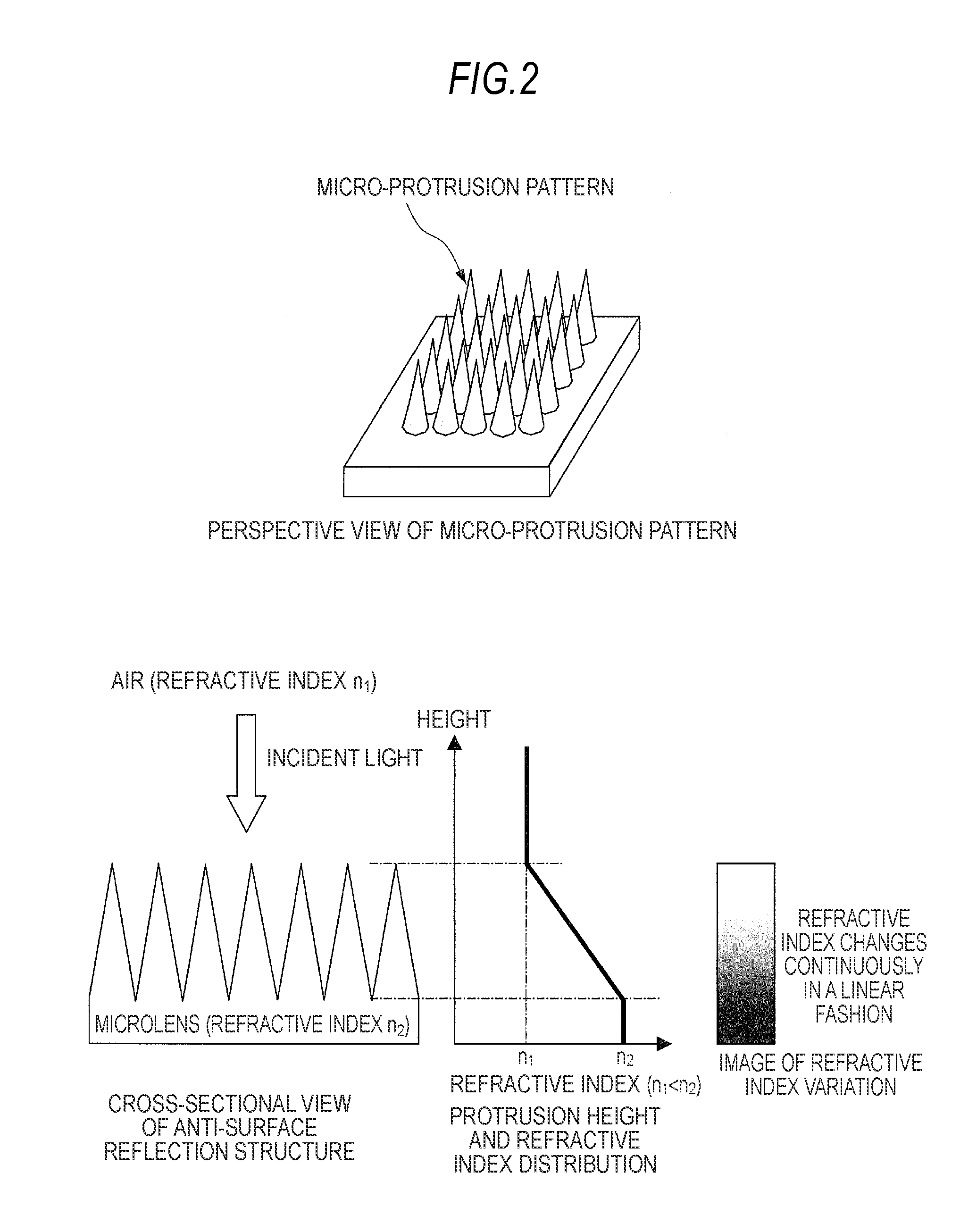
[0094]An example of a first fabrication method of an anti-reflection structure according to a first embodiment of the present invention will be described with reference to the cross-sectional views and SEM images shown in FIG. 4.

[0095]As illustrated in (1) in FIG. 4, a target substrate 11 on which a micro-protrusion pattern is to be formed is prepared.

[0096]As the target substrate 11, a silicon oxide film, a silicon nitride film, a silicon oxynitride, and the like may be used. Such a film may be applicable to an inorganic passivation film which is formed below a color filter of a solid-state imaging device, for example.

[0097]Subsequently, as illustrated in (2) in FIG. 4, a resin film 12 having micro-particles (not shown) dispersed therein is formed on a surface of the target substrate 11. The resin film 12 may be formed by preparing a resin serving as a base material of the resin film 12 and a solvent...

second embodiment

2. Second Embodiment

First Example of Second Fabrication Method of Anti-Reflection Structure

[0126]Next, a first example of a second fabrication method of an anti-reflection structure according to a second embodiment of the present invention will be described with reference to the cross-sectional views shown in FIGS. 5 and 6.

[0127]As illustrated in (1) in FIG. 5, micro-particles 13 are arranged on a surface of a target substrate 11.

[0128]For example, a solvent (not shown) having the micro-particles 13 dispersed therein is formed into a film form on the surface of the target substrate 11 so that the micro-particles 13 are arranged on the surface of the target substrate 11.

[0129]Specifically, the solvent (not shown) having the micro-particles 13 dispersed therein is applied into a film form onto the surface of the target substrate 11 by a coating method, and the solvent is then evaporated, whereby only the micro-particles 13 are arranged on the surface of the target substrate 11.

[0130]E...

third embodiment

3. Third Embodiment

Example of First Fabrication Method of Solid-State Imaging Device

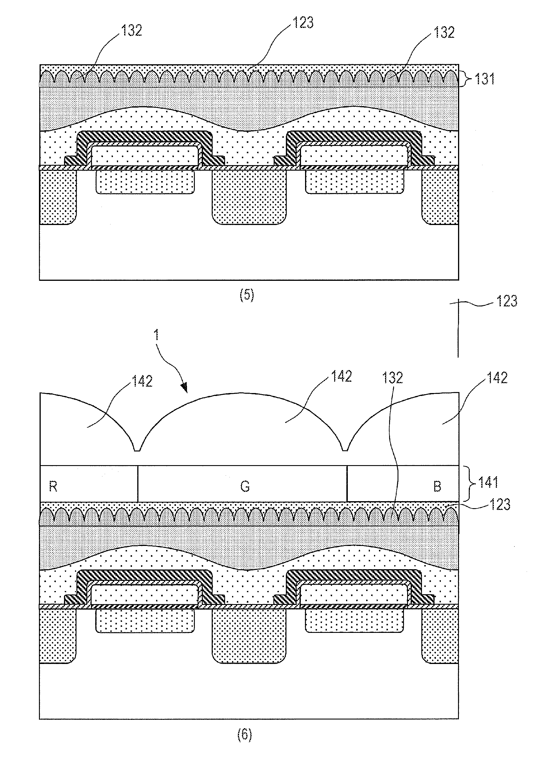
[0201]An example of a first fabrication method of a solid-state imaging device according to a third embodiment of the present invention will be described with reference to the cross-sectional views of FIGS. 12 to 13.

[0202]As illustrated in (1) in FIG. 12, a photoelectric conversion portion 22 that converts an incident light to signal charges is formed in a semiconductor substrate 21. Moreover, a vertical charge transfer portion 23 that reads and transfers the signal charges from the photoelectric conversion portion 22 is formed in the semiconductor substrate 21. At the same time, a horizontal charge transfer portion (not shown) that transfers and outputs the signal charges transferred from the vertical charge transfer portion 23 in the horizontal direction is formed. On the vertical charge transfer portion 23 (the horizontal charge transfer portion as well) of the semiconductor substrate 21, a transf...


PUM

PropertyMeasurementUnit
heightaaaaaaaaaa
heightaaaaaaaaaa
heightaaaaaaaaaa

Abstract

A fabrication method of an anti-reflection structure includes the steps of: forming a resin film having micro-particles dispersed therein on a surface of a substrate; forming a protrusion dummy pattern on the resin film by etching the resin film using the micro-particles in the resin film as a mask while gradually etching the micro-particles; and forming a protrusion pattern on the surface of the substrate by etching back the surface of the substrate together with the resin film having the protrusion dummy pattern formed thereon, and transferring a surface shape of the protrusion dummy pattern formed on a surface of the resin film to the surface of the substrate.

Description

BACKGROUND OF THE INVENTION[0001]1. Field of the Invention[0002]The present invention relates to a solid-state imaging device, a fabrication method thereof, an imaging apparatus, and a fabrication method of an anti-reflection structure.[0003]2. Description of the Related Art[0004]In solid-state imaging devices, it is necessary for a photoelectric conversion portion to convert incident light to electrical signals while preventing reflection of the incident light in order to increase conversion efficiency of the photoelectric conversion portion performing photoelectric conversion on the incident light.[0005]Therefore, it is desirable to decrease the light components reflected from the interfaces as much as possible.[0006]In solid-state image sensors, a light-condensing stacked structure is formed to efficiently condense light. In this case, since the stacked layers of different materials produce an interface at which a difference in refractive indices is large, there occurs an optical...

Claims


Application Information

Patent Timeline
Patent Type & Authority Applications(United States)
IPC IPC(8): H01L31/0236H01L21/302H01L31/18H01L31/0232
CPCG02B1/118H01L21/0335H01L21/31144Y02E10/50H01L27/14685H01L31/0236H01L27/1462H01L31/02363G02F1/133528
Inventor MAEDA, KENSAKUKOIKE, KAORUSASAKI, TOHRUTATSUMI, TETSUYA
Owner SONY CORP
Why Eureka
Try Eureka