

Clamp ring for wafer and method of manufacturing semiconductor apparatus
- Summary
- Abstract
- Description
- Claims
- Application Information
AI Technical Summary
Benefits of technology
Problems solved by technology
Method used
Image

Examples
Embodiment Construction
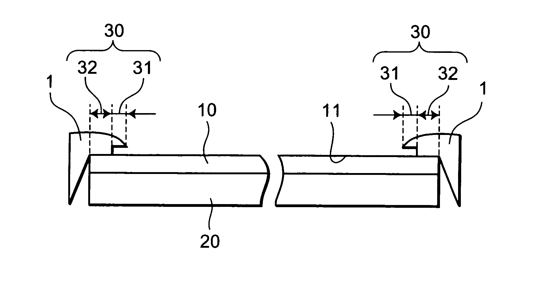
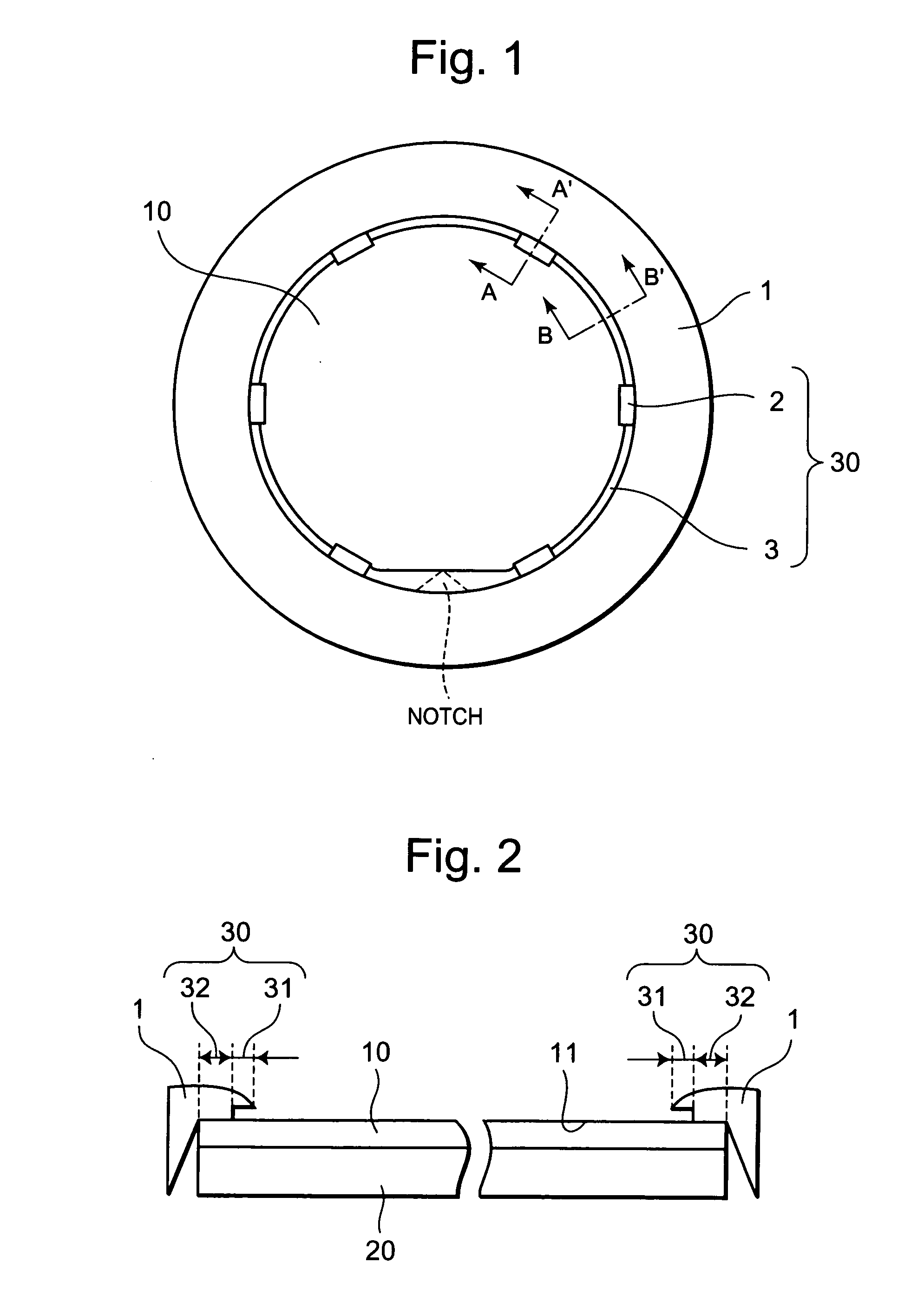
[0026]FIG. 1 is a top view illustrating a state when a wafer 10 is fixed by a clamp ring according to a exemplary embodiment, and FIG. 2 is a sectional view illustrating the state when the wafer 10 is fixed by the clamp ring according to the exemplary embodiment. The clamp ring is used to fix a wafer in a film depositing process. In the exemplary embodiment, a sputtering process is described as an example of the film depositing process.
[0027]As shown in FIG. 1, the clamp ring includes a clamp ring main body 1 and a fixing part 30.
[0028]The clamp ring main body 1 is ring-shaped. The inner periphery of the clamp ring main body 1 has a shape corresponding to the outer periphery of the wafer 10.
[0029]The fixing part 30 is a part for pressing the wafer 10. The fixing part 30 extends from the inner periphery of the clamp ring main body 1 towards the inside (the center of a wafer when the wafer is fixed). The fixing part 30 is provided to correspond to the entire inner periphery of the cla...
PUM
 Abstract
Description
Claims
Application Information