Etch system

Inactive Publication Date: 2009-06-04
APPLIED MATERIALS INC
View PDF2 Cites 367 Cited by
  • Summary
  • Abstract
  • Description
  • Claims
  • Application Information

AI Technical Summary

Problems solved by technology

Although many, if not all of these different processes, are performed on a single wafer when making an integrated circuit, th

Method used


Image

  • Etch system
  • Etch system
  • Etch system

Examples


Embodiment Construction

[0026]Semiconductor processing systems are described for achieving a desired process efficiency and / or substrate throughputs.

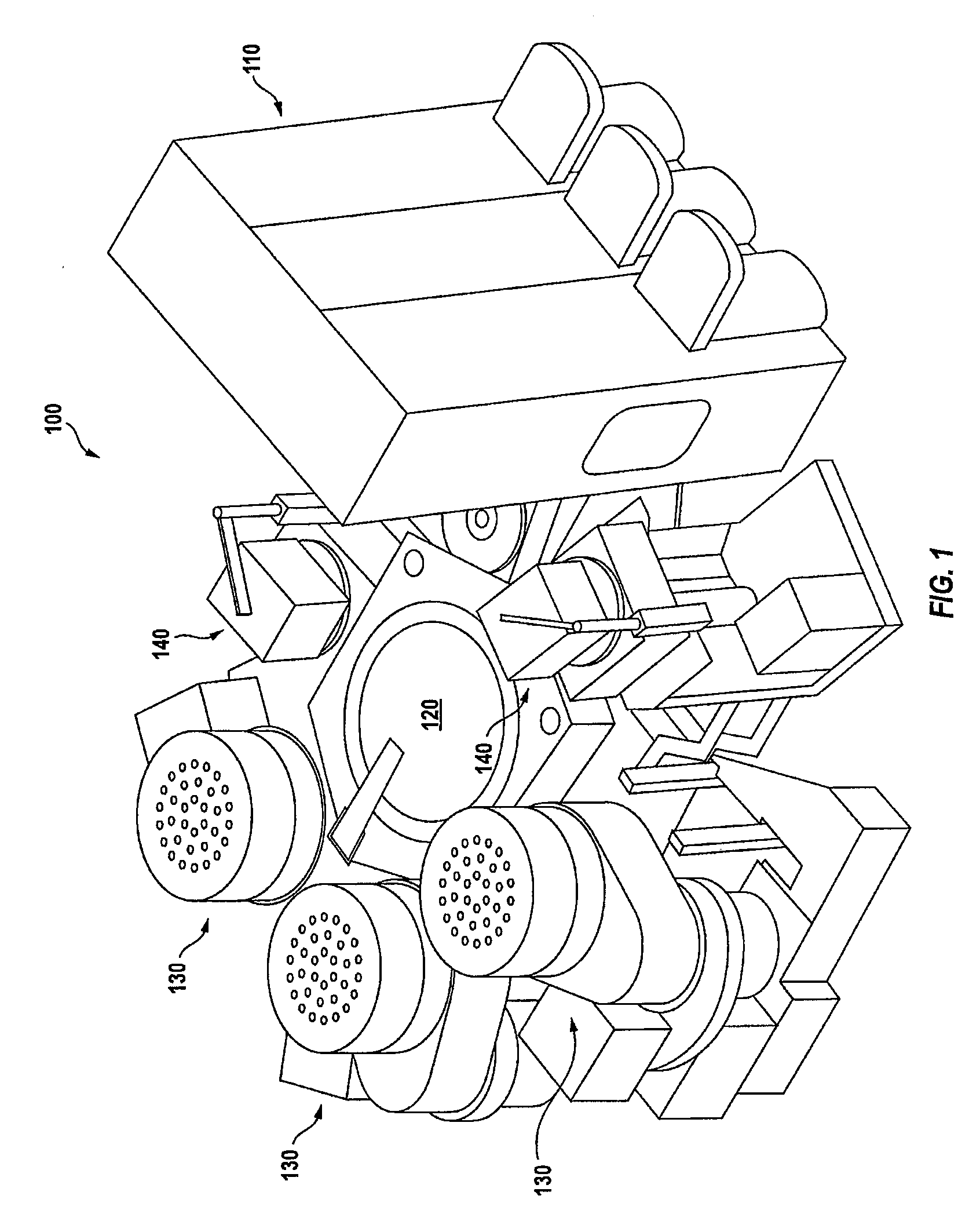
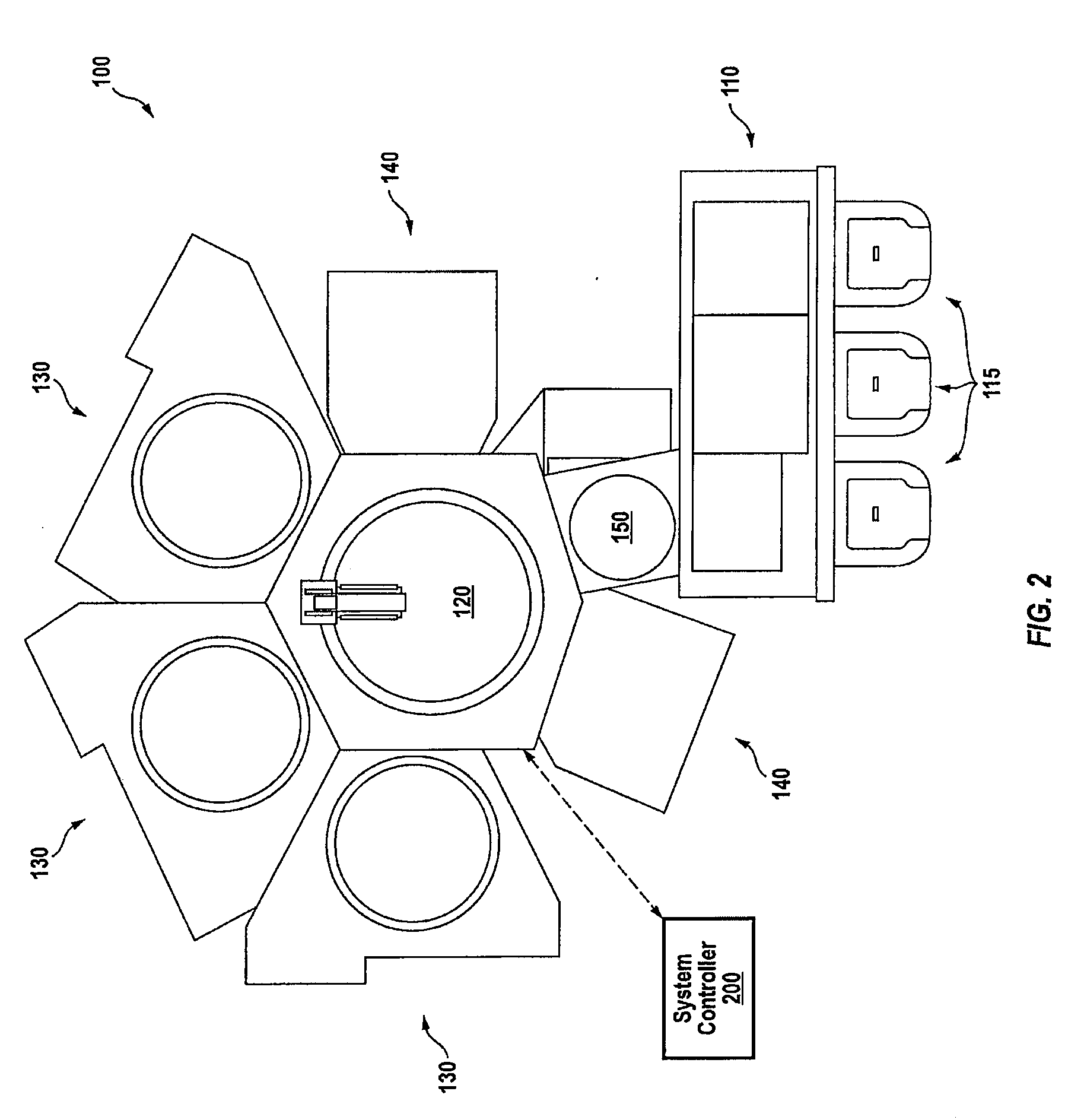
[0027]According to embodiments of the present invention, a semiconductor processing system includes a factory interface, a central transfer chamber, a first number of etch chambers, and a second number of post-etch treatment chambers. The factory interface is coupled to the transfer chamber and the transfer chamber is coupled to the first number of etch chambers and the second number of post-etch treatment chambers. The first number of etch chambers are configured to etch a substrate at about a first processing time. The second number of post-etch treatment chambers are configured to process the substrate at about a second processing time. The ratio of the first number to the second number is substantially proportional to a ratio of the first processing time to the second processing time.

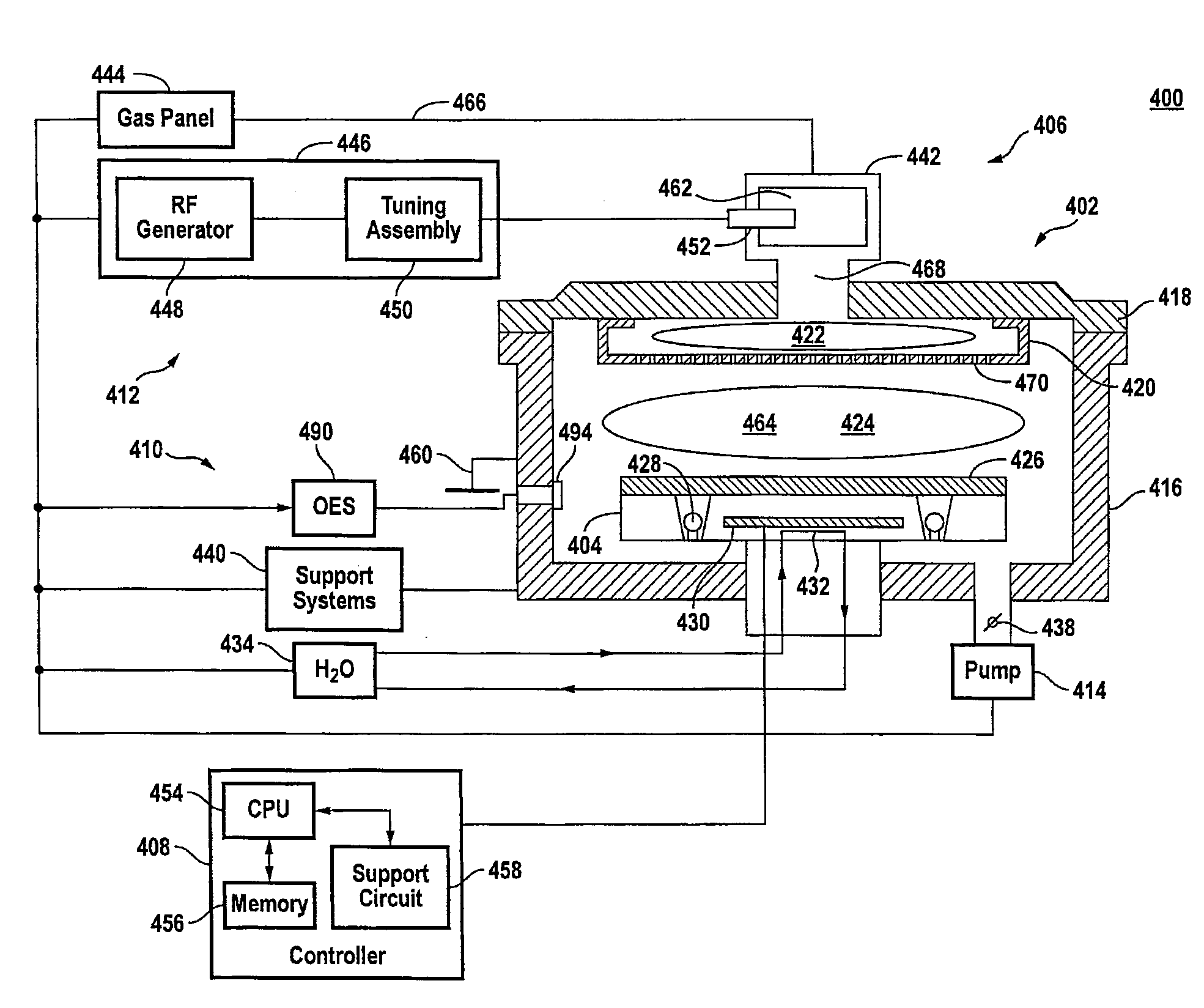
[0028]FIG. 1 is a schematic drawing of an exemplary semiconductor process...


PUM

PropertyMeasurementUnit
Timeaaaaaaaaaa
Timeaaaaaaaaaa
Timeaaaaaaaaaa

Abstract

A semiconductor processing system includes a factory interface. A central transfer chamber is coupled to the factory interface. A first number of etch chambers are coupled to the central transfer chamber. The first number of etch chambers are configured to etch a substrate at about a first processing time. A second number of post-etch treatment chambers are coupled to the central transfer chamber. The second number of post-etch treatment chambers are configured to process the substrate at about a second processing time, wherein a ratio of the first number to the second number is substantially proportional to a ratio of the first processing time to the second processing time.

Description

CROSS-REFERENCES TO RELATED APPLICATIONS[0001]The present application claims benefit under 35 USC 119(e) of U.S. provisional Application No. 60 / 992,283 filed on Dec. 4, 2007, entitled “Etch System,” the content of which is incorporated herein by reference in its entirety. This application is related to co-assigned U.S. Patent Publication No. 2006 / 0289384 to Pavel et al, filed Aug. 28, 2006, and entitled “METHOD AND APPARATUS FOR PERFORMING HYDROGEN OPTICAL EMISSION ENDPOINT DETECTION FOR PHOTORESIST STRIP AND RESIDUE REMOVAL.” This application is also related to co-assigned U.S. Patent Publication No. 2007 / 0077767 to Jin et al., filed Aug. 14, 2006, and titled “METHOD OF PLASMA ETCHING OF HIGH-K DIELECTRIC MATERIALS.” The entire contents of both related applications are hereby incorporated by reference for all purposes.BACKGROUND[0002]Embodiments of the present invention relate in general to semiconductor processing systems and in particular to etch systems used to process semicondu...

Claims


Application Information

Patent Timeline
IPC IPC(8): H01L21/306
CPCH01J37/32357H01J37/32449H01J37/32935H01L21/67276H01L21/67069H01L21/67207H01J37/32972
Inventor LEE, CHANGHUNEATON, BRADMA, DIANA X.
Owner APPLIED MATERIALS INC
Why Eureka
Try Eureka