Mechanical isolation for MEMS devices

a technology of mechanical isolation and mems devices, applied in the direction of semiconductor devices, semiconductor/solid-state device details, electrical apparatus, etc., can solve the problems of capacitive sensor problems, devices are subject to stress, and affect the performance of mems devices

Active Publication Date: 2009-07-02
HONEYWELL INT INC
View PDF7 Cites 44 Cited by
  • Summary
  • Abstract
  • Description
  • Claims
  • Application Information

AI Technical Summary

Problems solved by technology

Non-inertial and mechanical stresses due to die mounting can affect the performance of MEMS devices.
Additionally, the devices are subject to stress during wire bonding.
Packaging stress causes problems for capacitive sensors that require stable geometry for stable output.
Making wire bonds at th

Method used


Image

  • Mechanical isolation for MEMS devices
  • Mechanical isolation for MEMS devices
  • Mechanical isolation for MEMS devices

Examples


Embodiment Construction

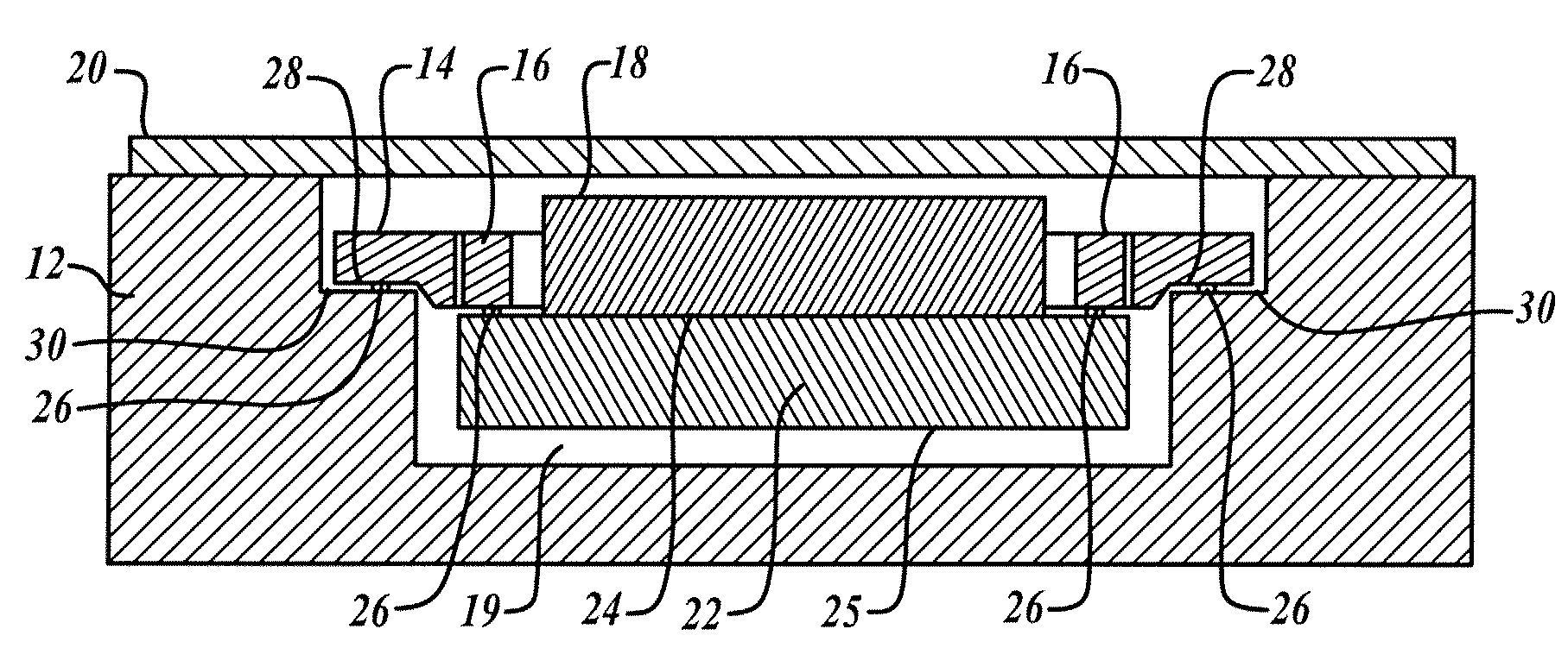
[0018]FIG. 1 shows a device 10 according to an embodiment of the present invention. The device 10 includes a package 12 and an isolator 14. The isolator 14 includes perimeter isolation structures 16, which can be tines, and a receptacle 17 for receiving a top cover 18 of an associated MEMS device (not shown). The isolator may be fabricated from a non-conductive, semi-conductive or fully conductive material.

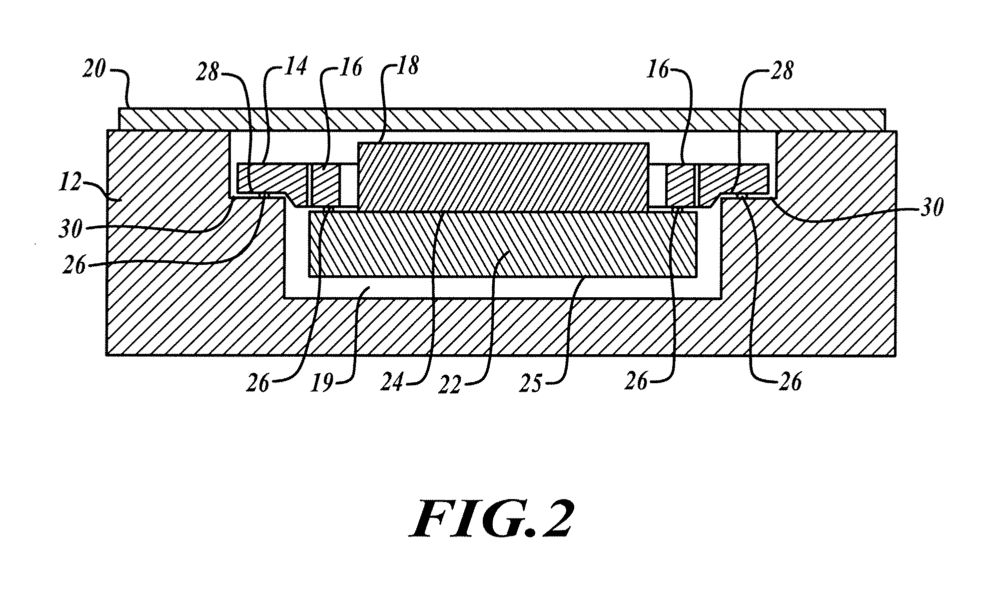
[0019]FIG. 2 is a cross-section through AA of the device 10 of FIG. 1. A package cover 20 can be included as advantageous depending on the MEMS device and the intended working environment. A die 22 is suitably attached to a MEMS device (not shown) on a top side 24 of the die 22. The top side 24 of the die 22 is attached by an electrically conductive attachment device 26, such as gold bumps, to a bottom side 28 of the isolator 14. The package includes a stepped recess 19 for receiving the MEMS device, die 22, and isolator 14, with the bottom side 28 of the isolator 14 attached by e...


PUM


Abstract

A device according to the present invention includes a MEMS device supported on a first side of a die. A first side of an isolator is attached to the first side of the die. A package is attached to the first side of the isolator, with at least one electrically conductive attachment device attaching the die to the isolator and attaching the isolator to the package. The isolator may include isolation structures and a receptacle.

Description

[0001]Microelectromechanical systems (MEMS) devices or computer chips are often mounted on dies. Non-inertial and mechanical stresses due to die mounting can affect the performance of MEMS devices. Additionally, the devices are subject to stress during wire bonding. Packaging stress causes problems for capacitive sensors that require stable geometry for stable output. Making wire bonds at the package level also increases the cost of manufacture because each part must be handled separately, and increases the chance of damage to the assembly.[0002]MEMS devices are often mounted to another structure in order to measure inertial forces experienced by the structure. Directly mounted MEMS devices are exposed to stresses applied by the structure, which leads the MEMS device to produce inaccurate measurements.SUMMARY OF THE INVENTION[0003]A device and method for isolation of MEMS devices is provided by an embodiment of the present invention. A device according to one aspect of the present i...

Claims


Application Information

Patent Timeline
IPC IPC(8): H01L23/495H01L21/52
CPCB81B7/0048B81B2207/012H01L2924/0002H01L2924/00
Inventor FOSTER, MICHAELJAFRI, IJAZESKRIDGE, MARKZHOU, SHIFANG
Owner HONEYWELL INT INC
Why Eureka
Try Eureka