Anisotropic stress generation by stress-generating liners having a sublithographic width

a stress-generating line and anisotropic technology, applied in the direction of semiconductor devices, semiconductor/solid-state device details, electrical apparatus, etc., can solve problems such as disadvantages

Inactive Publication Date: 2009-07-23
GLOBALFOUNDRIES INC
View PDF4 Cites 31 Cited by
  • Summary
  • Abstract
  • Description
  • Claims
  • Application Information

AI Technical Summary

Benefits of technology

[0055]forming another field effect transistor on the semiconductor substrate, wherein the another field effect transistor includes another gate line, another source side metal semiconductor alloy region, and another drain side metal semiconductor alloy region; and
[0056]forming a stress-generating layer comprising the stress-generating material and abutting the another gate line, the another source side metal semiconductor alloy

Problems solved by technology

However, applying such a tensile stress along a longitudinal direction would produce an advantageou

Method used


Image

  • Anisotropic stress generation by stress-generating liners having a sublithographic width
  • Anisotropic stress generation by stress-generating liners having a sublithographic width
  • Anisotropic stress generation by stress-generating liners having a sublithographic width

Examples


first embodiment

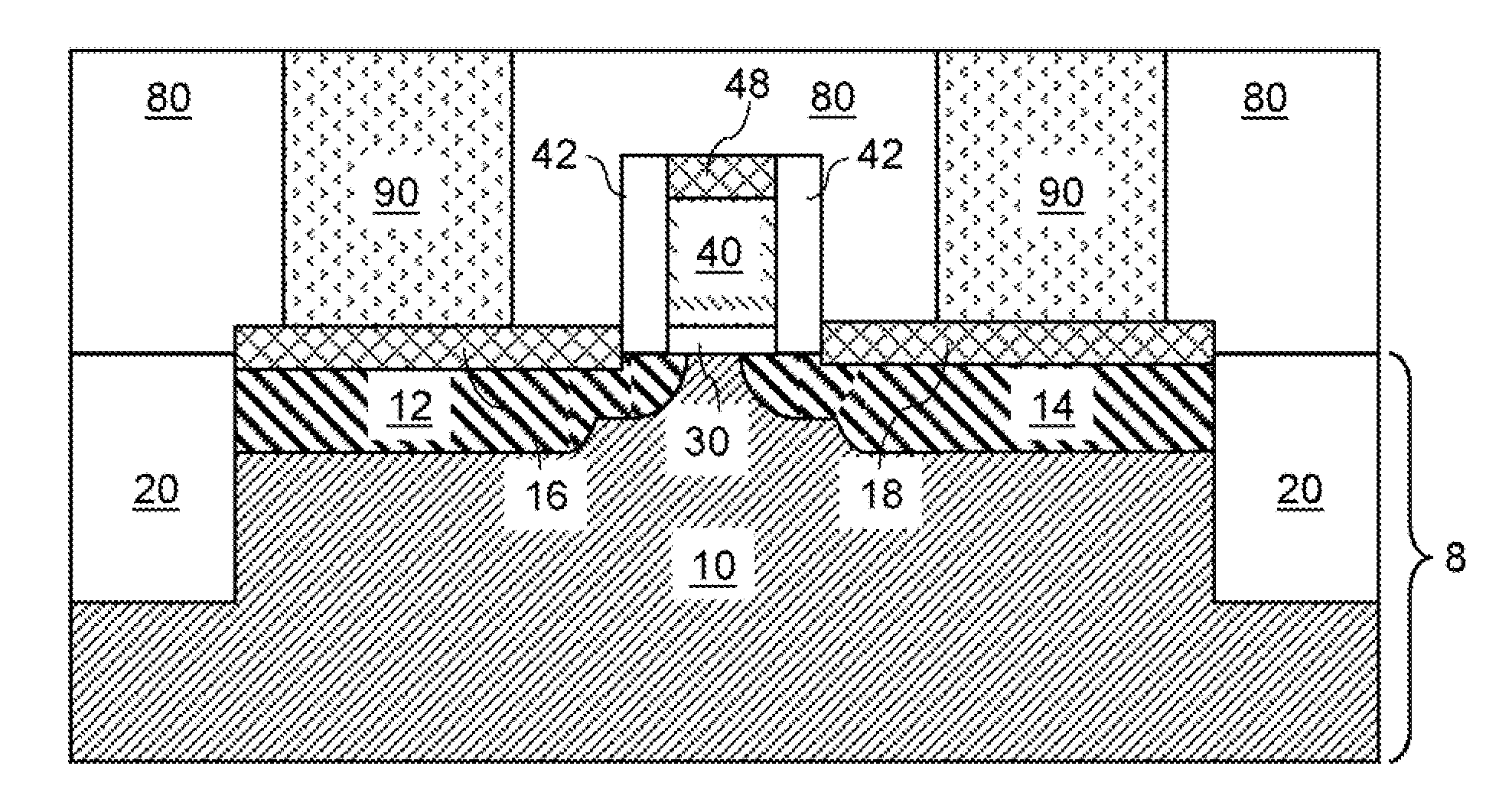
[0086]In the present invention, a PFET and an NFET, each having a structure substantially the same as the first exemplary semiconductor structure, are formed on the same semiconductor substrate. Such an implementation is beneficial if both the PFET and the NFET benefits from a transverse stress of the same type.

[0087]For example, the semiconductor substrate may be a (001) silicon substrate, and the channel of the PFET and the channel of the NFET are along one of crystallographic orientations. The direction of the channel refers to the direction of the current flow in the channel of the transistor. As discussed above, both the PFET and the NFET benefits from a transverse tensile stress if the substrate is a (001) silicon substrate and the channels are along one of the crystallographic orientations.

[0088]In general, some combinations of semiconductor materials in the semiconductor substrate, substrate orientations, and channel orientations provide a system comprising a PFET and an N...

second embodiment

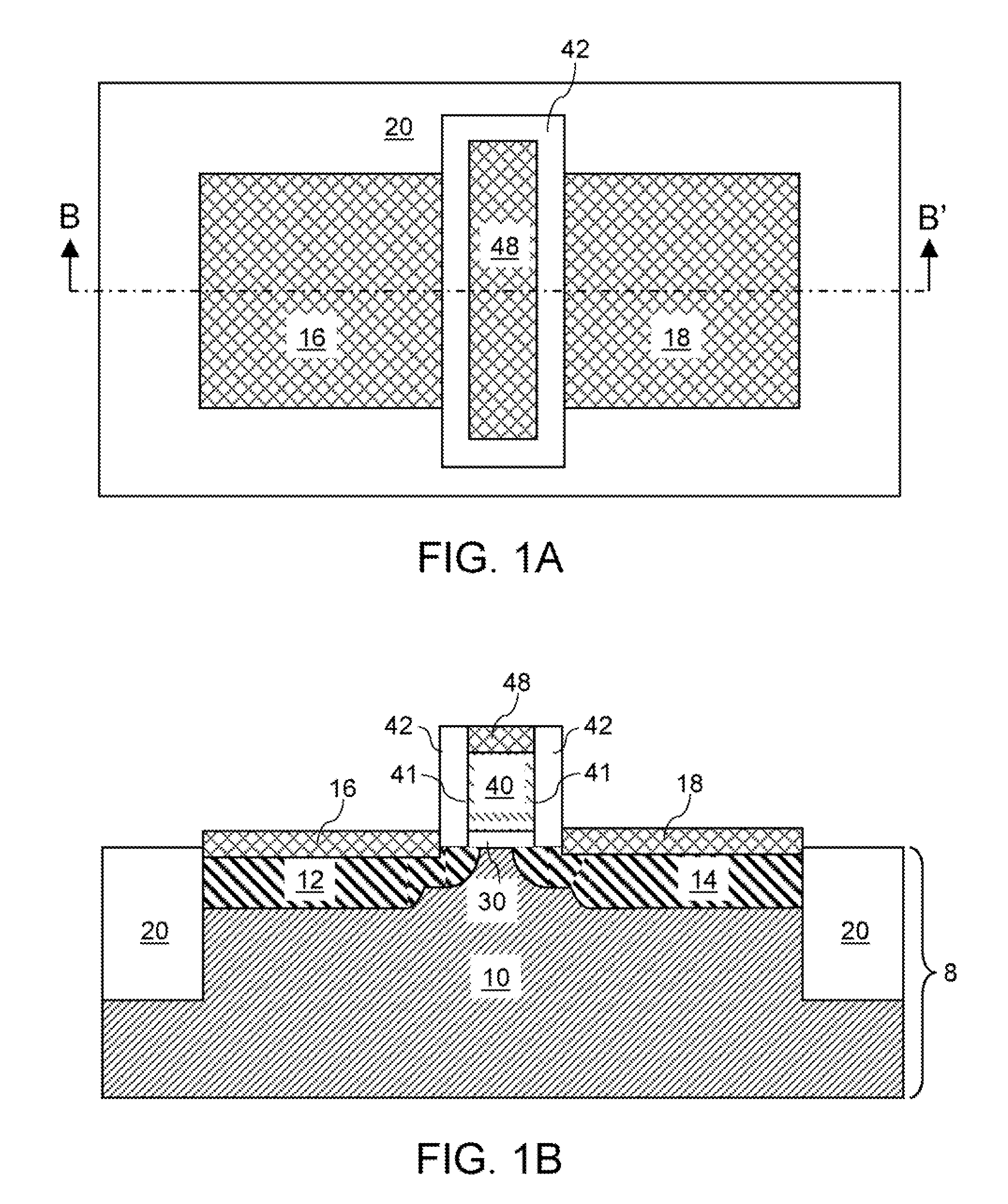
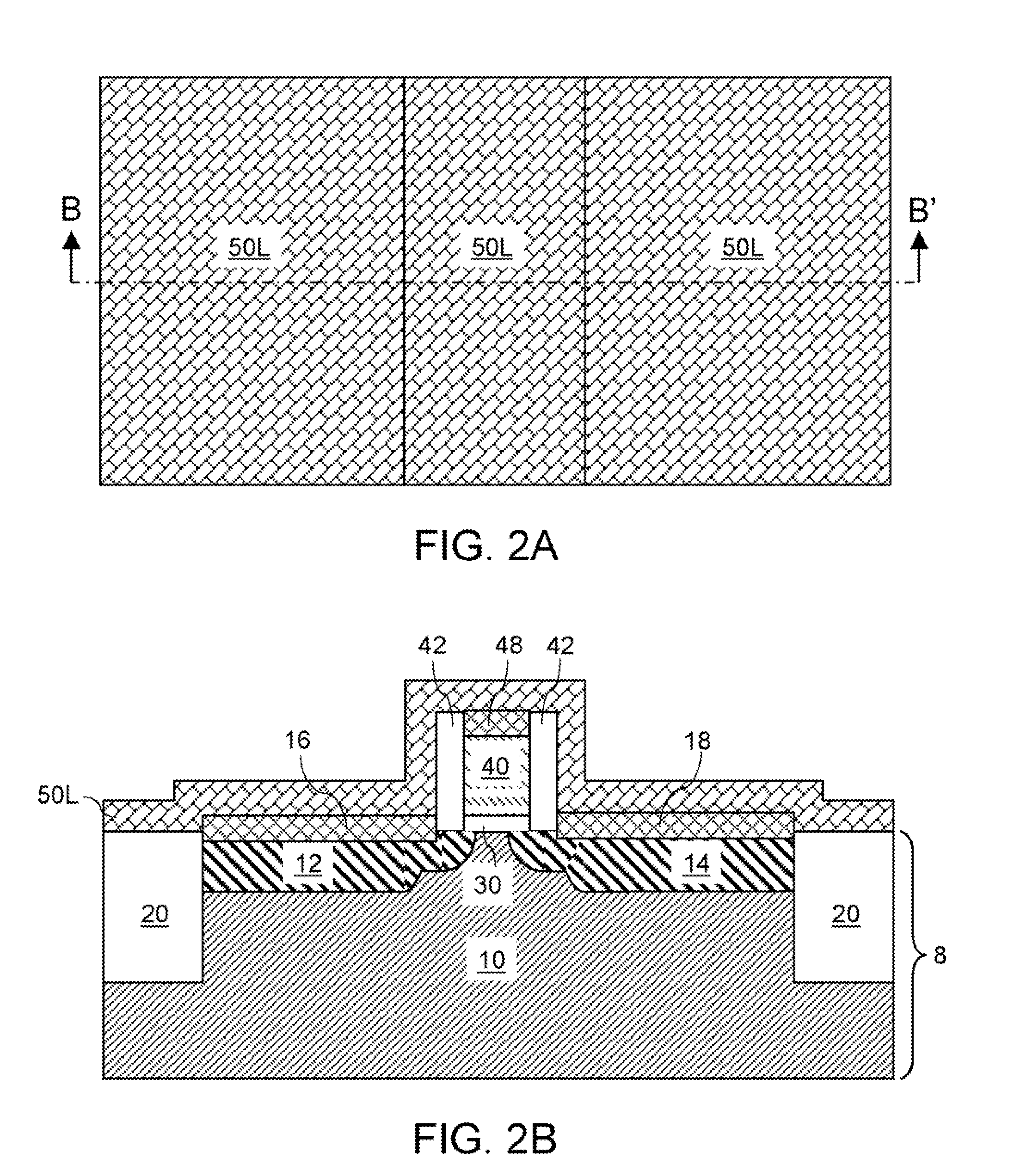
[0090]According to the present invention, such additional longitudinal stress as well as a transverse stress is provided in a second exemplary semiconductor structure. In the second exemplary semiconductor structure, formation of a plurality of linear stress-generating stripes is prevented on one type of field effect transistor. Instead, a stress-generating layer comprising the stress-generating material and abutting a gate line, a source side metal semiconductor alloy region, and a drain side metal semiconductor alloy region provides both the longitudinal stress and the transverse stress of the same type, i.e., compressive or tensile.

[0091]The second exemplary semiconductor structure is formed on the same semiconductor substrate concurrently with the formation of the first exemplary semiconductor structure. Specifically, a first exemplary semiconductor structure containing a first field effect transistor of one conductivity type (i.e., a PFET or an NFET) as shown in FIGS. 4A and 4B...

third embodiment

[0096]According to the present invention, any stress generated by the stress-generating material employed elsewhere on the same semiconductor substrate is eliminated in a third exemplary semiconductor structure, which is disjoined from any structure comprising the stress-generating material. In the third exemplary semiconductor structure, formation of a plurality of linear stress-generating stripes or a stress-generating layer comprising the stress-generating material is prevented on one type of field effect transistors.

[0097]The third exemplary semiconductor structure is formed on the same semiconductor substrate concurrently with the formation of the first exemplary semiconductor structure. Specifically, a first exemplary semiconductor structure containing a first field effect transistor of one conductivity type (i.e., a PFET or an NFET) as shown in FIGS. 3A and 3B and a third exemplary semiconductor structure containing a third field effect transistor of the opposite type (i.e., ...


PUM


Abstract

A protruding structure having a linear edge is formed on a substrate. The protruding structure may be a gate line of a field effect transistor. A stress-generating liner is deposited on the substrate. A non-photosensitive self-assembling block copolymer layer containing at least two immiscible polymeric block components is deposited on the stress-generating liner, and is annealed to allow phase separation of immiscible components. The polymeric resist is developed to remove at least one of the at least two polymeric block components, which formed a pattern of nested lines due to the linear edge of the protruding structure. Linear nanoscale stripes are formed in the polymeric resist which is self-aligning and self-assembled. The stress-generating layer is patterned into linear stress-generating stripes having a sublithographic width. The linear stress-generating stripes provide a predominantly uniaxial stress along their lengthwise direction, providing an anisotropic stress to an underlying semiconductor device.

Description

FIELD OF THE INVENTION[0001]The present invention relates generally to semiconductor devices for integrated circuits, and more particularly to a metal oxide semiconductor field effect transistor (MOSFET) structure under an anisotropic stress generated by a stress-generating liner having a sublithographic width, and methods for manufacturing the same.BACKGROUND OF THE INVENTION[0002]Performance of semiconductor devices may be enhanced by increasing carrier (electron or hole) mobility in some semiconductor devices such as a metal oxide semiconductor field effect transistor (MOSFET). When stress is applied to the channel of a semiconductor transistor, the mobility of carriers, and as a consequence, the transconductance and the on-current of the transistor are altered from their original values for an unstressed semiconductor. This is because the applied stress and the resulting strain on the semiconductor structure within the channel affects the band gap structure (i.e., breaks the deg...

Claims


Application Information

Patent Timeline
IPC IPC(8): H01L21/336H01L29/78
CPCH01L21/31144H01L21/823807H01L21/823814H01L21/823871H01L29/7843H01L27/1203H01L29/665H01L29/7833H01L21/84H01L27/0924
Inventor CLEVENGER, LAWRENCE A.DORIS, BRUCE B.HUANG, ELBERT E.PURUSHOTHAMAN, SAMPATHRADENS, CARL J.
Owner GLOBALFOUNDRIES INC
Why Eureka
Try Eureka