Semiconductor memory device
- Summary
- Abstract
- Description
- Claims
- Application Information
AI Technical Summary
Benefits of technology
Problems solved by technology
Method used
Image
Examples
Embodiment Construction
[0034]Hereinafter, a semiconductor memory device in accordance with the present invention will be described in detail with reference to the accompanying drawings.
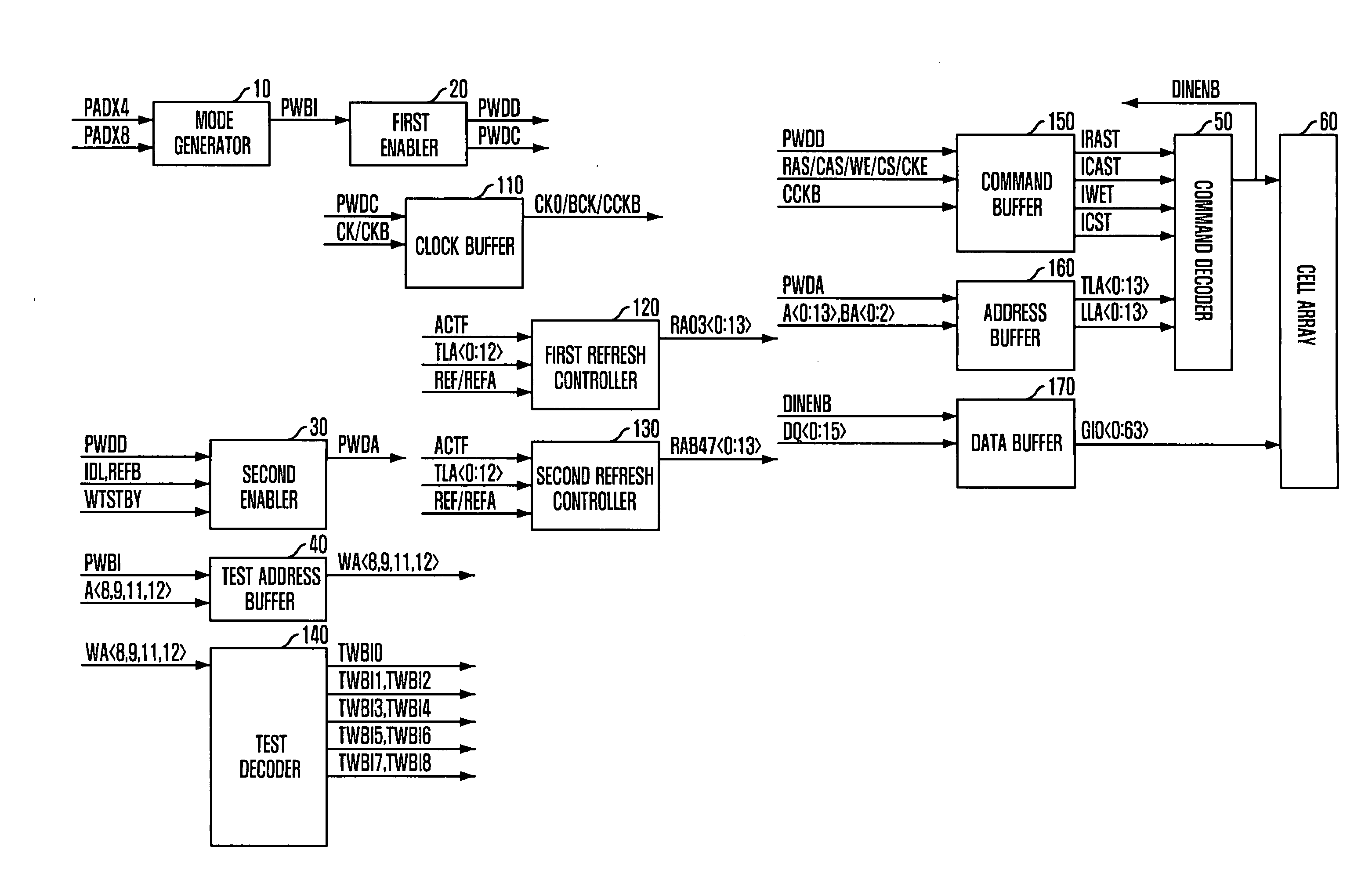
[0035]A wafer burn-in (WBI) mode is a test mode of detecting defects by applying a DC voltage to a word line or a bit line in a relatively short time (maximally, a few of seconds). In accordance with the present invention, however, even in a WBI mode performed at a wafer-level, it is possible to perform a built-in self-stress (BISS) test allowing a semiconductor memory device to be operated similarly to a test pattern carried out in a test during burn-in (TDBI) process. Unlike the case where a variety of test patterns and algorithms are implemented through a plurality of pads, a WBI mode test for detecting defects is performed using only a small number of pads generally. However, in the present invention, the BISS test for various tests is performed by implementing an algorithm and a test pattern performed in the TDBI proce...
PUM
 Abstract
Description
Claims
Application Information


