
Semiconductor memory device

a memory device and semiconductor technology, applied in the direction of instruments, coding, code conversion, etc., can solve the problems of increasing the number of operations to be tested, complex testing process of fabricated semiconductor memory devices, and complex design and fabrication of semiconductor memory devices, so as to reduce or eliminate the test time for operation.

Active Publication Date: 2011-09-22
SK HYNIX INC
View PDF14 Cites 6 Cited by
  • Summary
  • Abstract
  • Description
  • Claims
  • Application Information

AI Technical Summary

Benefits of technology

The BISS test significantly reduces the testing time for semiconductor memory devices, enhances productivity, and lowers fabrication costs by enabling efficient defect detection at the wafer-level without the limitations of traditional burn-in tests.

Problems solved by technology

This causes a design and fabrication of a semiconductor memory device to be complex, and also causes a testing process of the fabricated semiconductor memory device to be complex and difficult.
More specifically, the number of operations to be tested increases, and a testing procedure for each operation is also complicated.
The testing process of a semiconductor memory device with high capacity and integration degree requires a complex algorithm and much test time due to its complexity.
Accordingly, it takes a long time to test a semiconductor memory device using a method of accessing the semiconductor memory device from the outside and testing it by an automatic test equipment (ATE), which has been typically used.
Consequently, this typical method leads to a decrease in productivity of a semiconductor memory device as well as test efficiency.
Therefore, there is increasing difficulty in mass-producing a semiconductor memory device, and thus many attempts have been made to prevent a decrease in productivity.
Since the TDBI process is performed at a package level, excessive current consumption sometimes causes package balls to be melted to thereby damage a test equipment including a probe card, leading to an increase in test cost.
However, the TDBI process is not effective to reduce a test time notably.
However, a defect may occur in a unit cell of a semiconductor memory device in various circumstances besides read and write operations.
If a variety of test patterns and algorithms are incorporated in an internal circuit for BIST in consideration of such various circumstances, a total area of the semiconductor memory device may be unfavorably increased.
As described above, however, there is a disadvantage in that it takes a long time to test a semiconductor memory device in a TDBI process.

Method used


Image

  • Semiconductor memory device
  • Semiconductor memory device
  • Semiconductor memory device

Examples


Embodiment Construction

[0034]Hereinafter, a semiconductor memory device in accordance with the present invention will be described in detail with reference to the accompanying drawings.

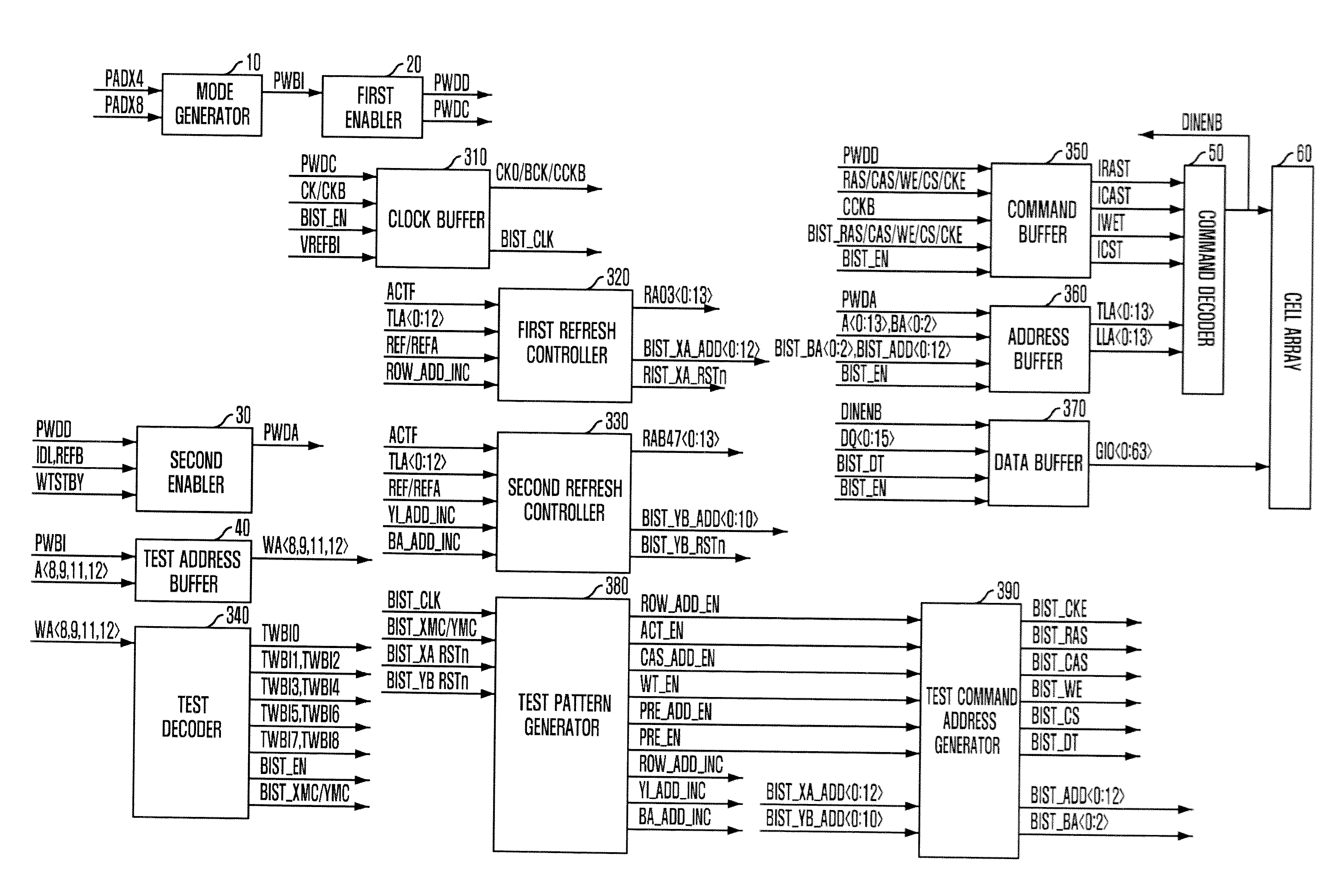
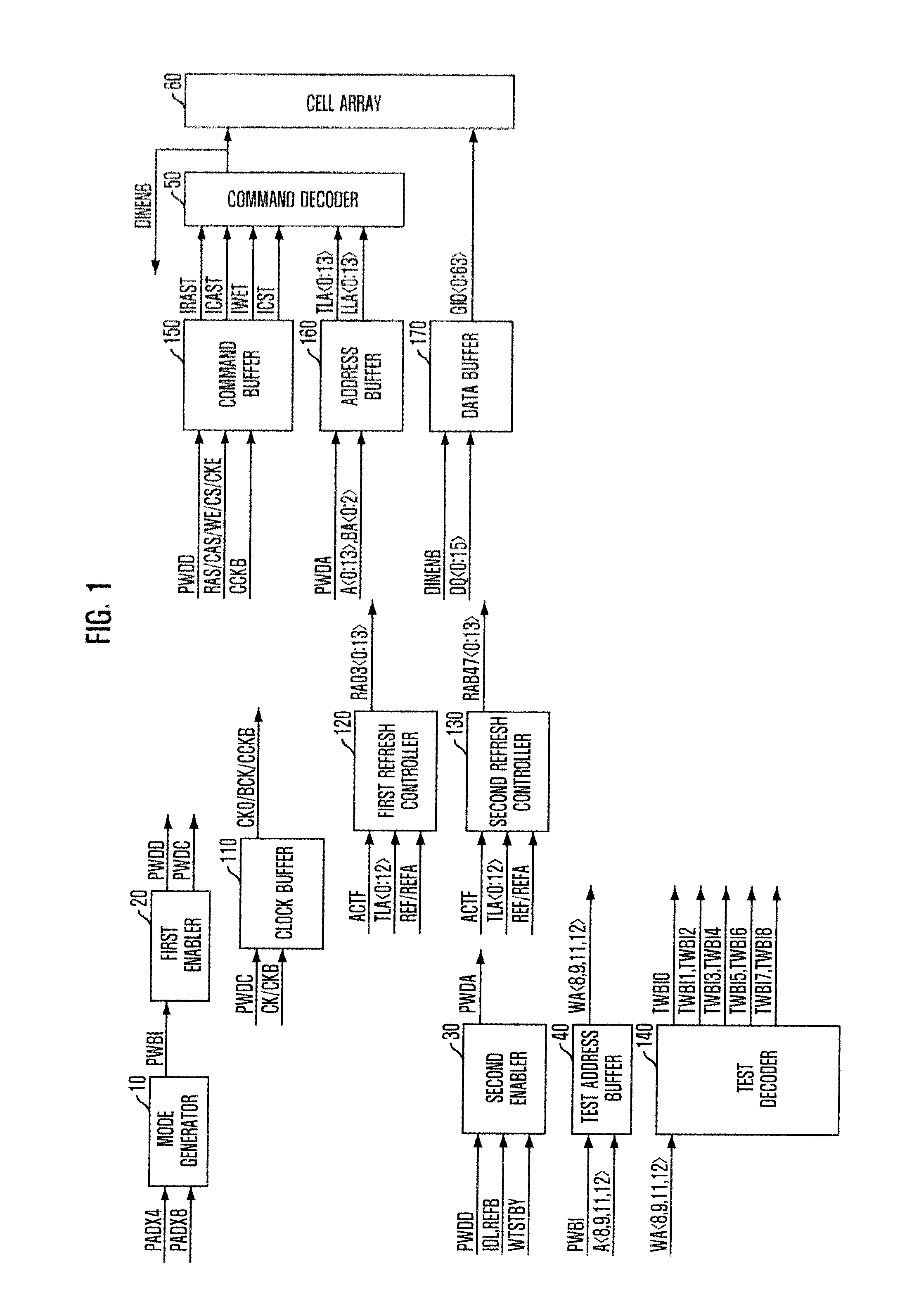
[0035]A wafer burn-in (WBI) mode is a test mode of detecting defects by applying a DC voltage to a word line or a bit line in a relatively short time (maximally, a few of seconds). In accordance with the present invention, however, even in a WBI mode performed at a wafer-level, it is possible to perform a built-in self-stress (BISS) test allowing a semiconductor memory device to be operated similarly to a test pattern carried out in a test during burn-in (TDBI) process. Unlike the case where a variety of test patterns and algorithms are implemented through a plurality of pads, a WBI mode test for detecting defects is performed using only a small number of pads generally. However, in the present invention, the BISS test for various tests is performed by implementing an algorithm and a test pattern performed in the TDBI proce...


PUM


Abstract

Semiconductor memory device includes a cell array including a plurality of unit cells; and a test circuit configured to perform a built-in self-stress (BISS) test for detecting a defect by performing a plurality of internal operations including a write operation through an access to the unit cells using a plurality of patterns during a test procedure carried out at a wafer-level.

Description

CROSS-REFERENCE TO RELATED APPLICATIONS[0001]The present invention claims priority of Korean patent application number 10-2008-0018761 filed on Feb. 29, 2008, which is incorporated by reference in its entirety.BACKGROUND OF THE INVENTION[0002]The present invention relates to a semiconductor memory device, and more particularly, to a semiconductor memory device that reduces a test time for operation of the semiconductor memory device with high capacity, and a testing method of the semiconductor memory device.[0003]In a system with a variety of semiconductor devices, a semiconductor memory device serves as a data storage. The semiconductor memory device outputs data according to addresses received from a data processor, e.g., a central processing unit (CPU), or stores data received from the data processor into memory cells selected by addresses.[0004]As the operating speed of the system increases and semiconductor integrated circuit technologies are advanced, semiconductor memory devi...

Claims


Application Information

Patent Timeline
Patent Type & Authority Applications(United States)
IPC IPC(8): G11C29/04G06F11/22
CPCG11C29/12G11C11/401G11C29/00
Inventor HUR, HWANGDO, CHANG-HOKO, JAE-BUMCHUNG, JIN-IL
Owner SK HYNIX INC
Learn More