Radiation imaging device
a technology of imaging device and radiation, which is applied in the direction of radioation controlled devices, instruments, television systems, etc., can solve the problem of limiting the size of each individual imaging element, and achieve the effects of reducing the formation of dead areas, high sensitivity, and high definition
- Summary
- Abstract
- Description
- Claims
- Application Information
AI Technical Summary
Benefits of technology
Problems solved by technology
Method used
Image
Examples
first embodiment
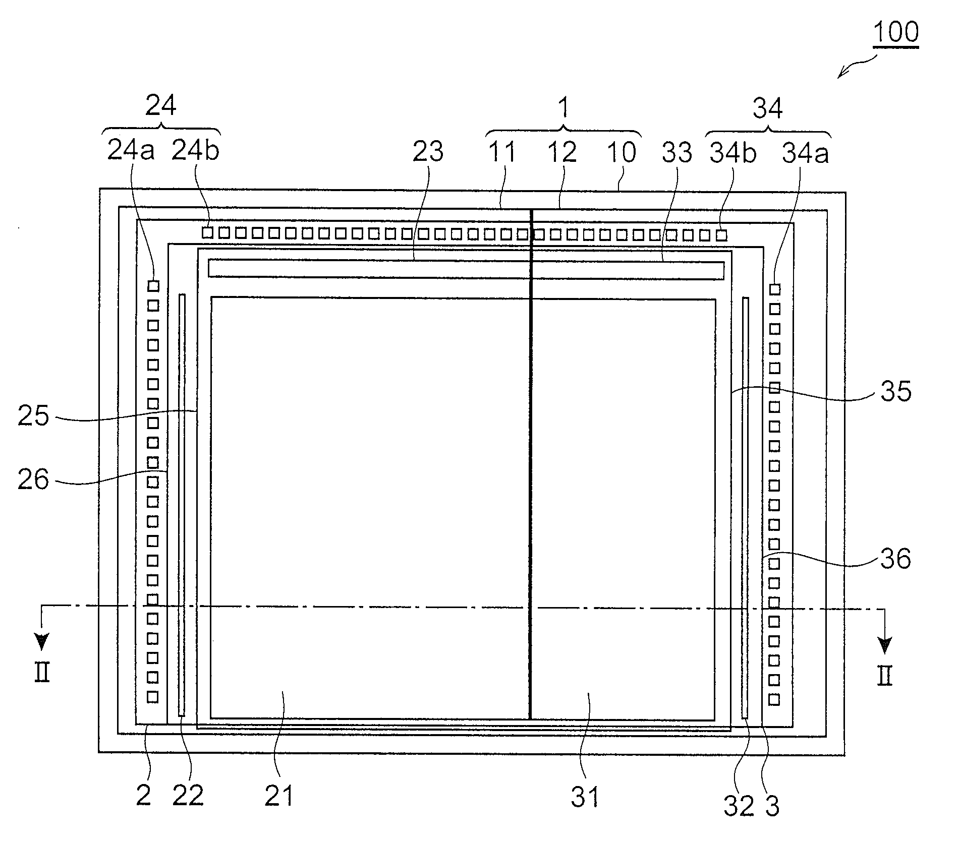
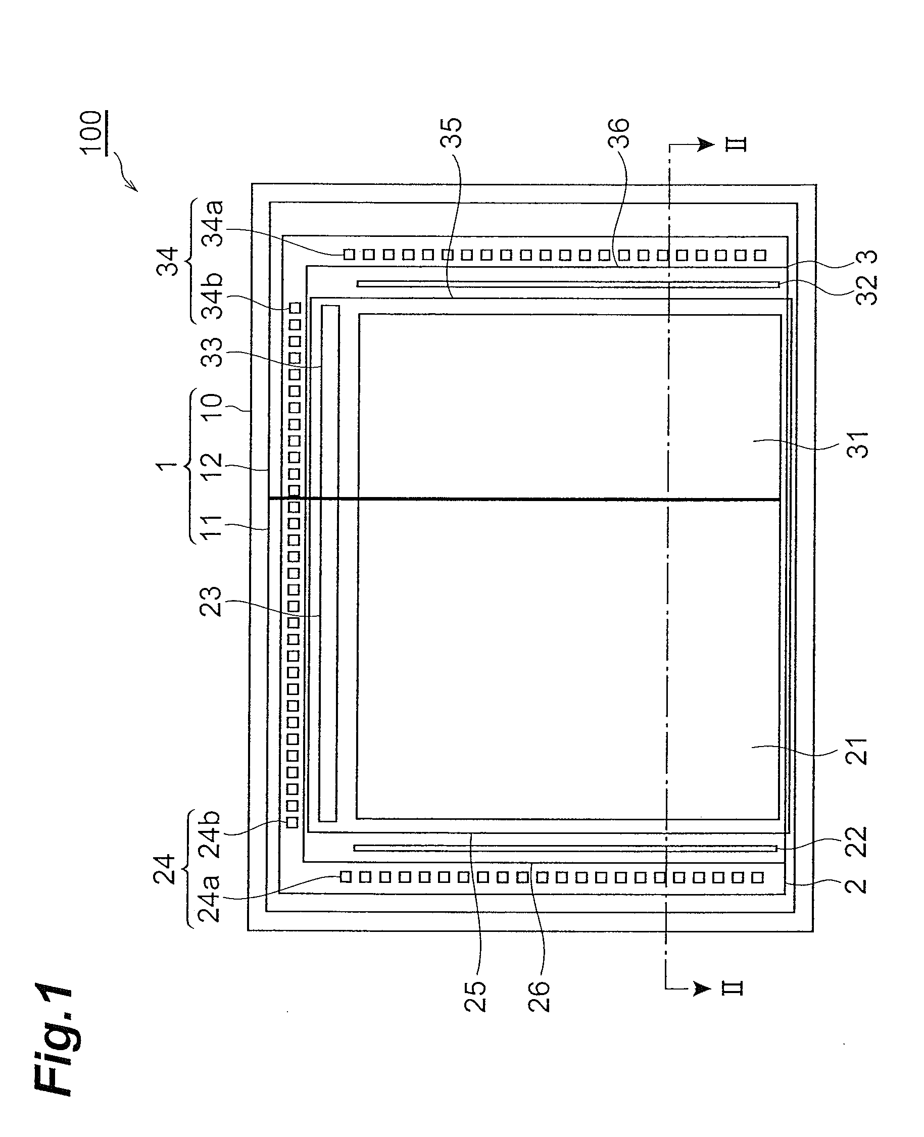
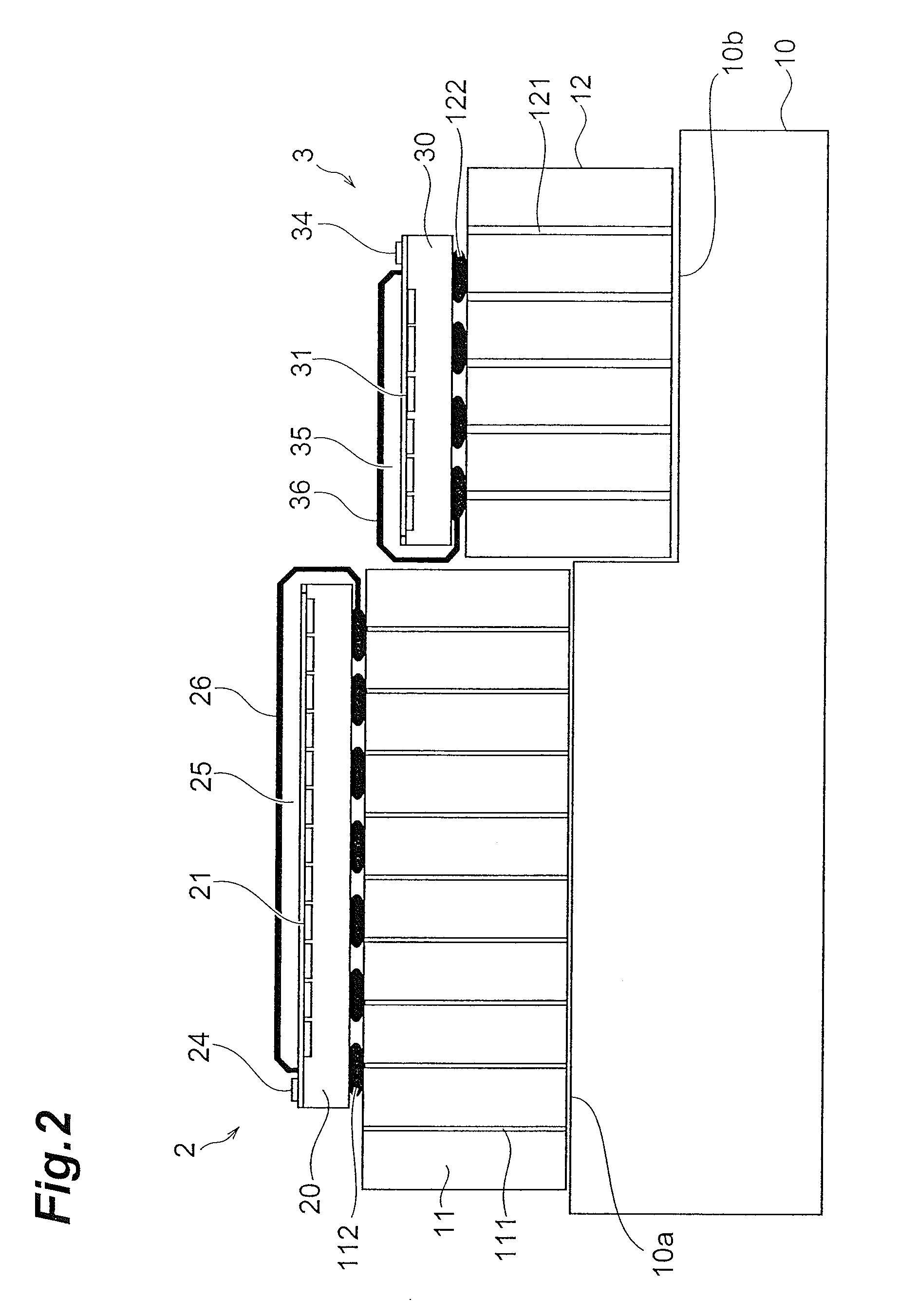
[0057]a radiation imaging device according to the present invention is shown in FIGS. 1 to 3. FIG. 1 is a front view as viewed from a radiation incident direction. FIG. 2 is a sectional view taken along line II-II of FIG. 1. FIG. 3 is an enlarged view of a boundary portion of radiation imaging elements of FIG. 2.
[0058]As shown in FIGS. 1 to 3, with the radiation imaging device 100, radiation imaging elements 2 and 3 are positioned in a stepped manner on a base 1. The radiation imaging elements 2 and 3 are MOS (Metal-Oxide Semiconductor) type image sensors formed on Si substrates 20 and 30, respectively, and are formed to rectangular plate-like shapes. Here, the Si substrate 20 has a size of 184 mm×2311 mm, the Si substrate 30 has a size of 96 mm×231 mm, and both have a thickness of 725 μm.
[0059]Each of photosensitive portions (photodetecting portions) 21 and 31, which are photodetecting regions, is positioned up to vicinities of two adjacent edges of each of the top surfaces of the ...
second embodiment
[0103]This embodiment is a modification example of the second embodiment and differs from the other embodiments in that a photosensitive portion 31a of a radiation imaging element 3a that is disposed at the back does not extend to the edge at the radiation imaging element 2 side and the interval from the photosensitive portion 31a to the end is set wider than that in the other embodiments.
[0104]Here, with the radiation imaging element 2 that is positioned at the front, in order to make small the dead area D resulting from the blocking of the other radiation imaging element 3a while securing imaging characteristics up to the end of the effective photodetecting region, the photosensitive portion 21 must be juxtaposed to the edge and the scintillator 25 must be formed at a substantially uniform thickness up to the end. Though for this purpose, it is preferable to form the scintillator 25 continuously at a substantially uniform thickness up to the side wall portion, the scintillator 25 ...
PUM
| Property | Measurement | Unit |
|---|---|---|
| thickness | aaaaa | aaaaa |
| size | aaaaa | aaaaa |
| size | aaaaa | aaaaa |
Abstract
Description
Claims
Application Information


