

Chip resistor and its manufacturing process
a technology of resistors and manufacturing processes, applied in the field of chip resistors, can solve the problems of circuit failure, excessive high temperature of resistor films ab>2/b>,
- Summary
- Abstract
- Description
- Claims
- Application Information
AI Technical Summary
Benefits of technology
Problems solved by technology
Method used
Image

Examples
first embodiment
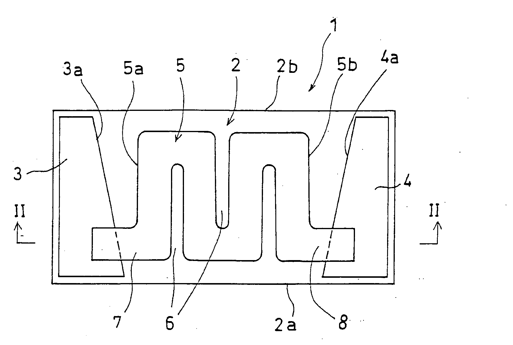
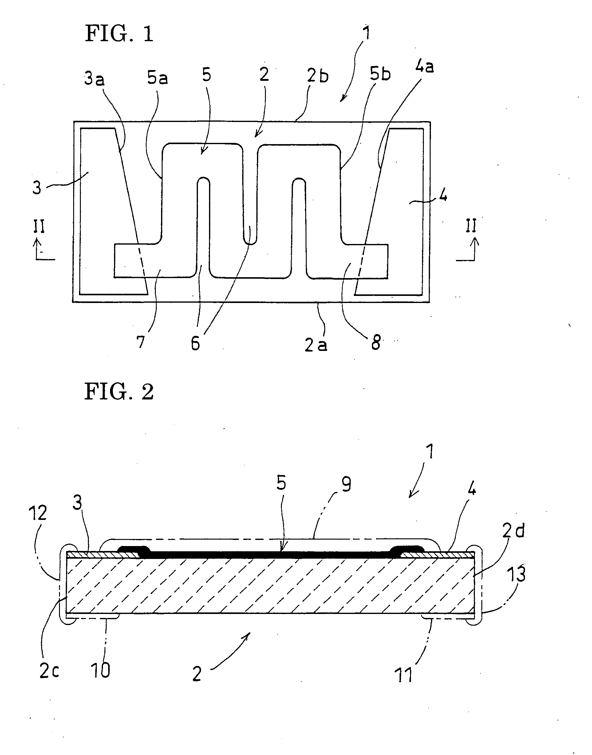
[0032]FIGS. 1 and 2 show a chip resistor 1 according to the present invention. The chip resistor 1 includes a rectangular chip substrate 2 made of a ceramic material. A pair of terminal electrodes 3 and 4 are formed by screen printing at longitudinally opposite ends of upper surface of the chip substrate 2. A resistor film 5 formed by screen printing is provided between the paired terminal electrodes 3 and 4 on the upper surface of the chip substrate 2. The resistor film 5 is formed with a plurality of grooves 6 extending inward from a pair of longitudinally extending edges of the resistor film. The grooves 6 may be formed in the above-described screen printing process or by trimming after the screen printing. With the provision of the grooves 6, the resistor film 5 extends in a meandering manner between an end 5a and another end 5b thereof in the longitudinal direction.
[0033]As shown in FIG. 1, the terminal electrodes 3 and 4 include inclined inner edges 3a and 4a, respectively. Sp...
second embodiment
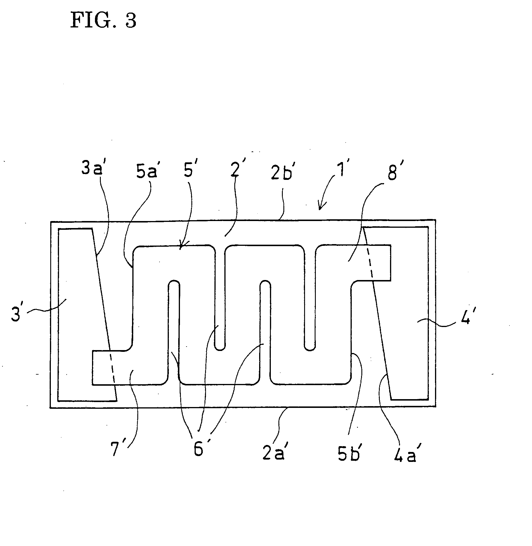
[0037]FIG. 3 shows a chip resistor 1′ according to the present invention.
[0038]The chip resistor 1′ includes a chip substrate 2′ in the form of an elongated rectangle made of a ceramic material, terminal electrodes 3′ and4′ formed by screen printing at longitudinally opposite ends of the upper surface of the chip substrate 2′, and a resistor film 5′ formed by screen printing between the paired terminal electrodes 3′ and 4′ on the upper surface of the chip substrate 2′ to extend longitudinally of the chip substrate. The resistor film 5′ is formed with a plurality of grooves 6′ extending inward from the longitudinal edges thereof, which may be formed in the screen printing process or by trimming after the screen printing. With the provision of the grooves, the resistor film 5 extends in a meandering manner between an end 5a′ and another end 5b′ thereof in the longitudinal direction.
[0039]The terminal electrode 3′ has an inner edge 3a′ which is inclined outwardly from a longitudinal si...
third embodiment
[0045]FIGS. 4-6 show a chip resistor 101 according to the present invention.
[0046]The chip resistor 101 includes an insulating substrate 102 made of a heat-resistant insulating material such as a ceramic material. The insulating substrate 102 is in the form of an elongated rectangle having a length L and a width W.
[0047]Terminal electrodes 103 for solder connection are provided on a pair of longitudinally-extending side surfaces 102′ of the insulating substrate 102 to extend along the side surfaces 102′.
[0048]A plurality of resistor films 104 (three resistor films in the example shown in the figure) are provided between the terminal electrodes 103 on the upper surface of the insulating substrate 102. The resistor films are arranged, in parallel with each other and spaced from each other in the longitudinal direction of the insulating substrate 102. Each of the resistor films 104 has opposite ends electrically connected to the terminal electrodes 103.
[0049]Each of the resistor films ...
PUM
| Property | Measurement | Unit |
|---|---|---|
| structure | aaaaa | aaaaa |
| length | aaaaa | aaaaa |
| width | aaaaa | aaaaa |
Abstract
Description
Claims
Application Information