Nonvolatile semiconductor memory device and method for manufacturing same

Active Publication Date: 2009-10-01
KIOXIA CORP
View PDF1 Cites 67 Cited by
  • Summary
  • Abstract
  • Description
  • Claims
  • Application Information

AI Technical Summary

Problems solved by technology

Thus, if the area of the stacked flash memory is increased to increase the capacity, the aforementioned conductive portions are also upsized, unfortunately increasing the resistance.
This makes it difficult to rapidly place each conductive portion at

Method used


Image

  • Nonvolatile semiconductor memory device and method for manufacturing same
  • Nonvolatile semiconductor memory device and method for manufacturing same
  • Nonvolatile semiconductor memory device and method for manufacturing same

Examples


first embodiment

[0024]At the outset, the invention is described.

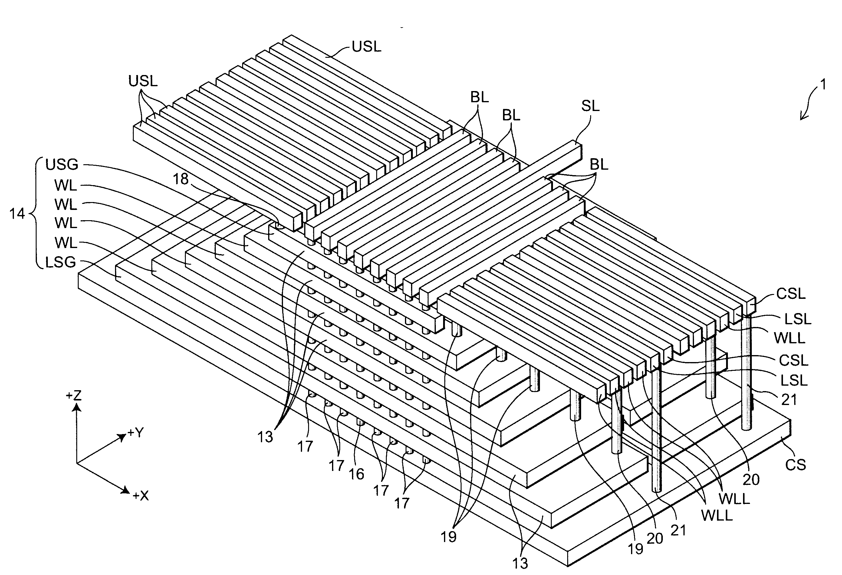
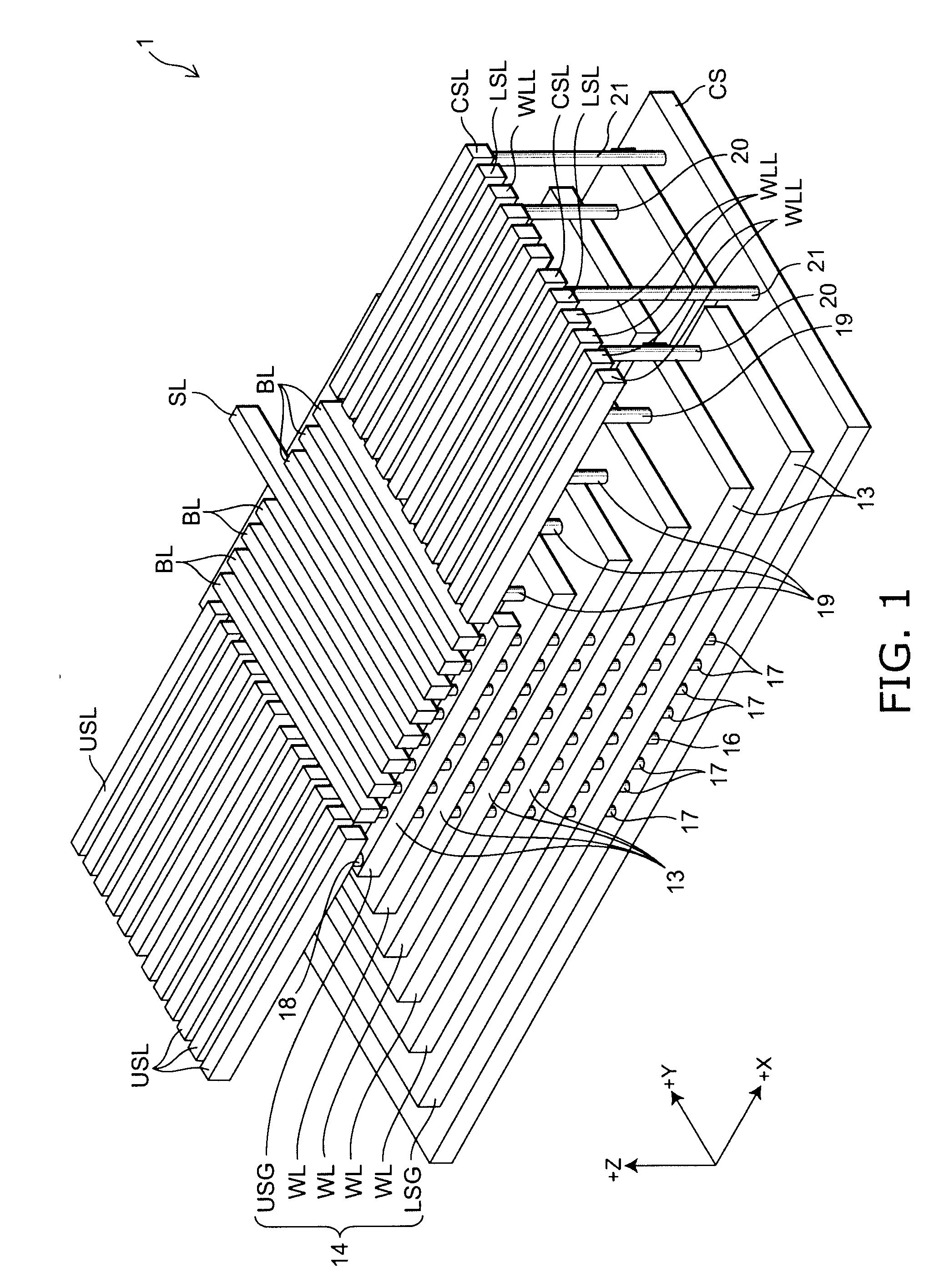
[0025]FIG. 1 is a perspective view illustrating a nonvolatile semiconductor memory device according to this embodiment.

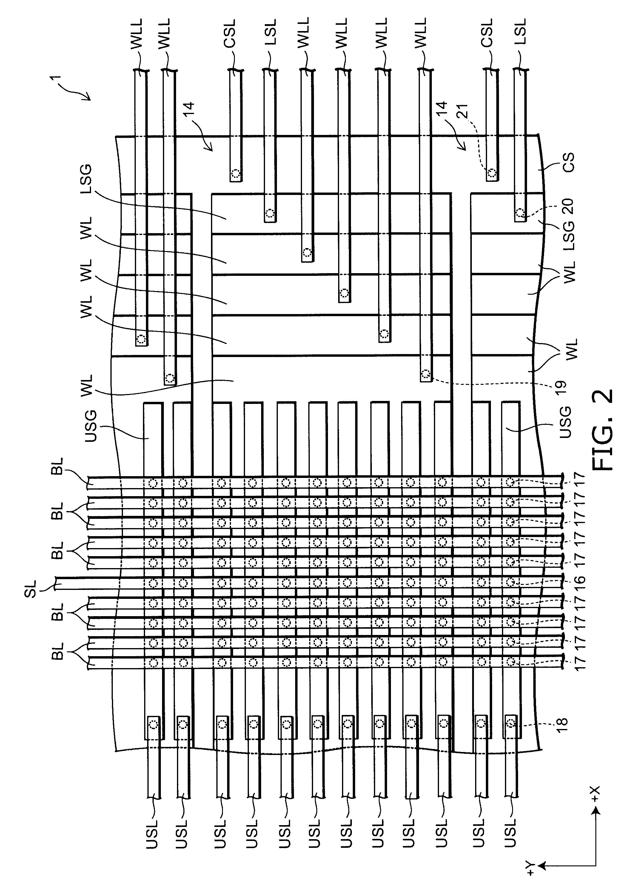
[0026]FIG. 2 is a plan view illustrating the nonvolatile semiconductor memory device according to this embodiment.

[0027]FIG. 3 is a cross-sectional view illustrating the nonvolatile semiconductor memory device according to this embodiment.

[0028]FIG. 4 is a perspective view illustrating one memory string in the nonvolatile semiconductor memory device according to this embodiment.

[0029]FIG. 5 is a cross-sectional view illustrating one memory cell in the nonvolatile semiconductor memory device according to this embodiment.

[0030]It is noted that in FIGS. 1 to 4, for clarity of illustration, only the conductive portions are shown, and the dielectric portions are not shown. Furthermore, in FIGS. 1 and 2, illustration of the silicon substrate 11 is also omitted. Similarly, in the other embodiments described later, the figures...

second embodiment

[0062]Next, the invention is described.

[0063]FIG. 6 is a plan view illustrating a nonvolatile semiconductor memory device according to this embodiment.

[0064]FIG. 7 is a cross-sectional view illustrating the nonvolatile semiconductor memory device according to this embodiment.

[0065]As shown in FIGS. 6 and 7, in the nonvolatile semiconductor memory device 2 according to this embodiment, an upper interconnect M extending in the X direction is provided above the shunt interconnect SL. The upper interconnect M is disposed for each stacked body 14 from immediately above the cell source interconnect CSL to immediately above the shunt interconnect SL. The +X-direction end portion of the upper interconnect M is connected to the cell source interconnect CSL through a via 32, and the −X-direction end portion is connected to the shunt interconnect SL through a via 33. The upper interconnect M is formed from a metal such as tungsten, aluminum, or copper. The configuration in this embodiment othe...

third embodiment

[0068]Next, the invention is described.

[0069]FIG. 8 is a plan view illustrating a nonvolatile semiconductor memory device according to this embodiment.

[0070]As shown in FIG. 8, in the nonvolatile semiconductor memory device 3 according to this embodiment, the shunt interconnect SL is divided for each stacked body 14. Furthermore, the upper interconnect M is provided for each stacked body 14. Hence, the device 3 includes as many upper interconnects M as the stacked bodies 14. Moreover, the cell source CS is also divided for each stacked body 14 into a plurality of portions along the Y direction. The plurality of portions of the cell source CS are arranged along the Y direction, and electrically isolated from each other. In each stacked body 14, the upper interconnect M is connected to the corresponding portion of the cell source CS through the shunt interconnect SL and the conductor pillar 16. The configuration in this embodiment other than the foregoing is the same as that in the ab...


PUM


Abstract

In a nonvolatile semiconductor memory device, a stacked body is formed by alternately stacking dielectric films and conductive films on a silicon substrate and a plurality of through holes extending in the stacking direction are formed in a matrix configuration. A shunt interconnect and a bit interconnect are provided above the stacked body. Conductor pillars are buried inside the through holes arranged in a line immediately below the shunt interconnect out of the plurality of through holes, and semiconductor pillars are buried inside the remaining through holes. The conductive pillars are formed from a metal, or low resistance silicon. Its upper end portion is connected to the shunt interconnect and its lower end portion is connected to a cell source formed in an upper layer portion of the silicon substrate.

Description

CROSS-REFERENCE TO RELATED APPLICATIONS[0001]This application is based upon and claims the benefit of priority from the prior Japanese Patent Application No. 2008-080526, filed on Mar. 26, 2008; the entire contents of which are incorporated herein by reference.BACKGROUND OF THE INVENTION[0002]1. Field of the Invention[0003]This invention relates to a nonvolatile semiconductor memory device with a plurality of dielectric films and electrode films alternately stacked on a substrate, and a method for manufacturing the same.[0004]2. Background Art[0005]Recently, to increase the density of flash memory, a technique for multilayering cells has been developed. In this technique, dielectric films and electrode films are alternately stacked on a substrate, and then through holes are simultaneously formed therein. A charge storage layer for retaining charge is formed on the inner surface of the through holes, and a columnar semiconductor pillar is buried inside each through hole. Thus, a memo...

Claims


Application Information

Patent Timeline
IPC IPC(8): H01L29/792H01L21/336
CPCH01L27/11551H01L23/528H01L27/11578H01L27/11556H01L2924/0002H10B41/20H10B43/20H10B41/27H01L2924/00H10B43/27H10B43/35H01L23/5226
Inventor MAEDA, TAKASHIIWATA, YOSHIHISA
Owner KIOXIA CORP
Why Eureka
Try Eureka