Method of manufacturing liquid crystal display device

Active Publication Date: 2009-10-01
UNIFIED INNOVATIVE TECH
View PDF8 Cites 2 Cited by
  • Summary
  • Abstract
  • Description
  • Claims
  • Application Information

AI Technical Summary

Problems solved by technology

However, in manufacturing an untwisted / aligned liquid crystal display device in which the molecular long axes of the liquid crystal molecules of a liquid crystal layer are aligned with the rubbing directions of the alignment films respectively formed on the opposed inner surfaces of a pair of substrates by performing rubbing treatment on the alignment films in parallel directions, the difference between the rubbing direction of each alignment film and the direction in which the film is worn by the screen influences the alignment of the liquid crystal molecules to disturb the alignment of the liquid crystal molecules.

Method used


Image

  • Method of manufacturing liquid crystal display device
  • Method of manufacturing liquid crystal display device
  • Method of manufacturing liquid crystal display device

Examples


first embodiment

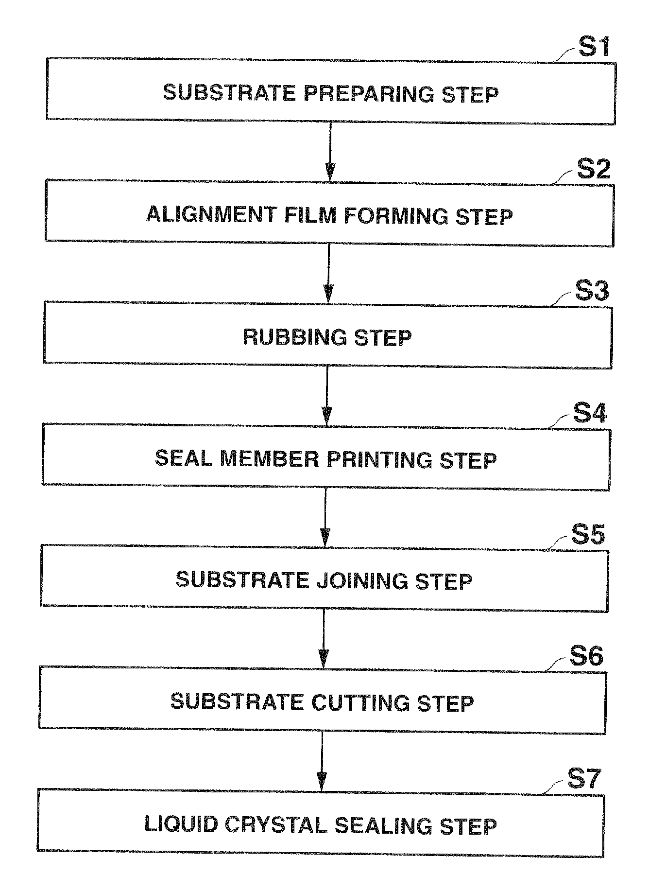
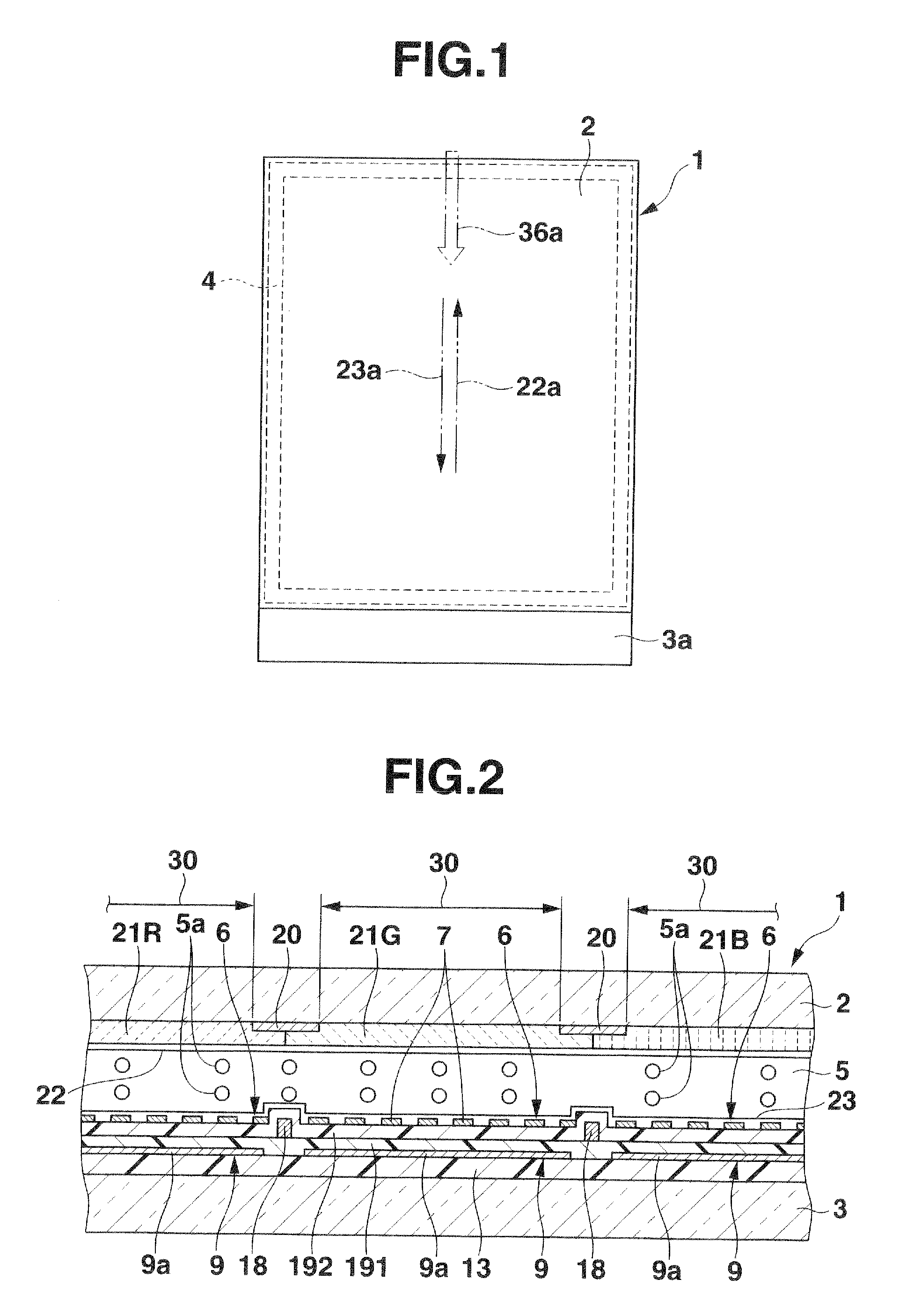
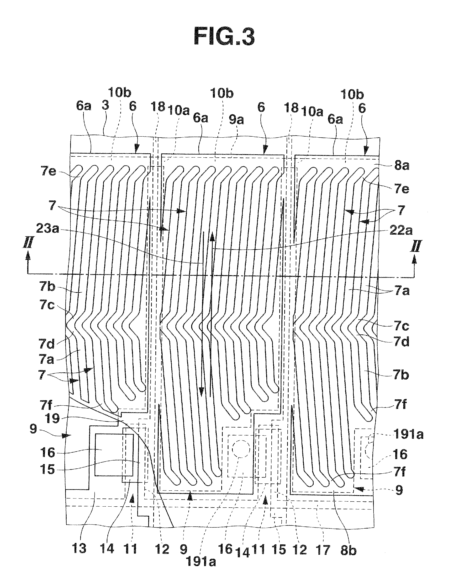
[0027]FIGS. 1 to 6 show the first embodiment of the present invention. FIG. 1 is a plan view of a liquid crystal display device to be manufactured. FIG. 2 is a sectional view taken along a line II-II of a liquid crystal display device according to the first embodiment in FIG. 3. FIG. 3 is an enlarged plan view of part of one of the substrates of the liquid crystal display device according to the first embodiment. FIG. 4 is an enlarged plan view showing the shapes of the first and second electrodes forming one pixel of the liquid crystal display device according to the first embodiment and the aligned state of liquid crystal molecules. FIG. 5 is a flowchart showing the manufacturing process of the liquid crystal display device according to the first embodiment. FIGS. 6A and 6B are sectional views each showing a printing method for a seal member on the liquid crystal display device according to the first embodiment.

[0028]A liquid crystal display device to be manufactured will be descr...

second embodiment

[0075]On the manufacturing method of the first embodiment, the seal member 4 is printed by moving the squeegee 36 in the same direction as the rubbing direction 23a of the alignment film 23 formed on the inner surface of one substrate 3. However, the seal member 4 can be printed by moving the squeegee 36 in a direction opposite to that in the first embodiment.

[0076]FIGS. 7A and 7B are views showing a seal member printing method according to the second embodiment of the present invention. In this embodiment, screen printing of a seal member 4 is performed by moving a squeegee 36 in a direction parallel and opposite to a rubbing direction 23a of an alignment film 23 formed on the inner surface of one substrate 3.

[0077]Note that this seal member printing method is the same as that in the first embodiment except that a moving direction 36a of the squeegee 36 is opposite to that in the first embodiment. Therefore, the same reference numerals as in the first embodiment denote the same par...


PUM

PropertyMeasurementUnit
shift angleaaaaaaaaaa
angleaaaaaaaaaa
angleaaaaaaaaaa

Abstract

A method of manufacturing a liquid crystal display device includes steps of preparing first and second substrates, forming alignment films on one surfaces of the first and second substrates, respectively, performing rubbing treatment on the alignment films, screen-printing a seal member on the one surface of the first substrate so as to surround a display area, and stacking the first and second substrates on each other while the first surfaces face to each other, with rubbing directions of the alignment films on the first and second substrates being parallel to each other, and joining the first and second substrates through the seal member by curing the seal member while the first and second substrates are bonded to each other through the seal member. The screen-printing is performed while a squeegee is moved in a direction parallel to the rubbing direction of the alignment film formed on the first substrate.

Description

CROSS-REFERENCE TO RELATED APPLICATIONS[0001]This application is based upon and claims the benefit of priority under 35 USC 119 of Japanese Patent Applications No. 2008-093156 filed on Mar. 31, 2008; and No. 2009-064476 filed on Mar. 17, 2009, the entire disclosure of which, including the description, claims, drawings, and abstract, is incorporated herein by reference in its entirety.BACKGROUND OF THE INVENTION[0002]1. Field of the Invention[0003]The present invention relates to a method of manufacturing a liquid crystal display device.[0004]2. Description of the Related Art[0005]In manufacturing a liquid crystal display device, after rubbing treatment is performed on alignment films respectively formed on the inner surfaces of a pair of substrates, a seal member for joining the pair of substrates is printed on the inner surface of one of the substrates by screen printing using a screen which masks a non-print area and a squeegee which is brought into contact with the screen and mov...

Claims


Application Information

Patent Timeline
Patent Type & Authority Applications(United States)
IPC IPC(8): G02F1/1337G02F1/1339H01J9/20
CPCG02F1/1339G02F1/1337
Inventor ARAI, NORIHIROMIZUSAKO, RYOTA
Owner UNIFIED INNOVATIVE TECH
Why Eureka
Try Eureka