Method and apparatus for manufacturing a device

Inactive Publication Date: 2006-05-30
BECTON DICKINSON & CO
View PDF7 Cites 132 Cited by
  • Summary
  • Abstract
  • Description
  • Claims
  • Application Information

AI Technical Summary

Benefits of technology

[0012]Accordingly, a primary object of the invention is to provide a method for efficiently manufacturing a micro-device from plastic or other materials.
[0013]Another object of the inven

Problems solved by technology

Although effective, the resulting microneedle devices are expensive to manufacture and are difficult to produce in large numbers.
The prior meth

Method used


Image

  • Method and apparatus for manufacturing a device
  • Method and apparatus for manufacturing a device
  • Method and apparatus for manufacturing a device

Examples


Example

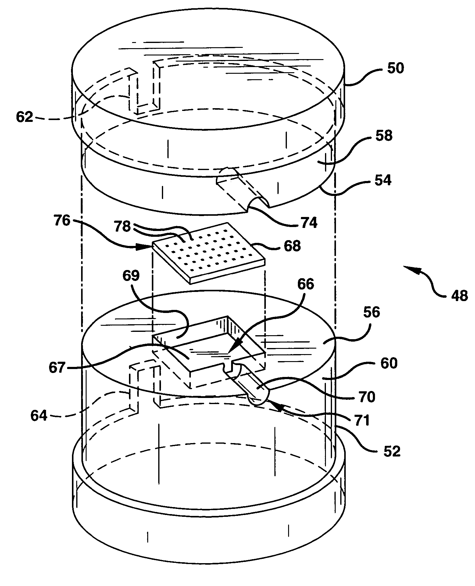
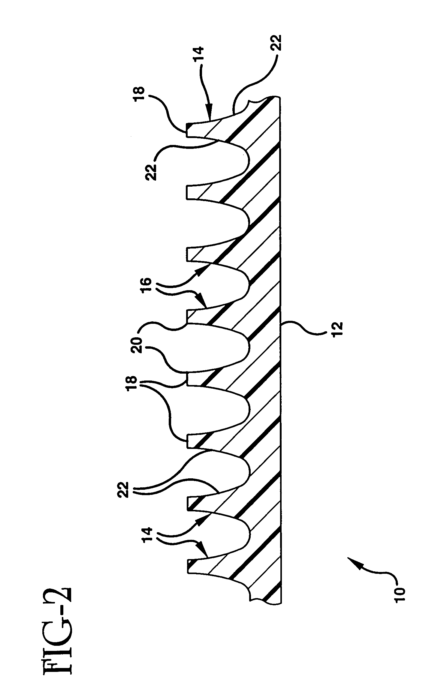
[0031]The present invention is directed to a method of manufacturing a micro-device, such as a medical device, having a plurality of micron or submicron size features. In one embodiment the micro-device is a microabrader device for preparing the skin for transdermally administering a substance to a patient or withdrawing a substance from the body of a patient. The method of the invention is able to mold a device having a plurality of micron size features, such as a microabrader device, from a polymeric material. The molding method, such as injection molding, is able to produce a high volume of the devices with micron or submicron size features in an inexpensive manner and with a high degree of consistency.

[0032]The devices formed by the method of the invention are preferably devices that have micron or submicron size details integrally molded therein. Examples of micro-devices that can be molded by the method and apparatus of the invention include medical and analytical devices havi...


PUM

PropertyMeasurementUnit
Lengthaaaaaaaaaa
Lengthaaaaaaaaaa
Densityaaaaaaaaaa

Abstract

A device, preferably a micro-device, is molded from a plastic material by injection molding, compression molding or embossing. A microabrader can be molded having microneedles for abrading the stratum corneum of the skin to form an abraded site in the tissue for enhancing drug delivery. The micro-device is molded using a mold assembly having a silicon molding surface. The silicon molding surface can include a recess corresponding to the desired shape and length of the microneedles. The silicon molding surface enables micron and submicron size features to be molded from polymeric materials without the polymeric material adhering to the mold surface. Micro-devices having molded features having micron and submicron dimensions can be rapidly produced without the use of a release agent.

Description

CROSS-REFERENCE TO RELATED APPLICATIONS[0001]This non-provisional application is a divisional of U.S. application Ser. No. 09 / 974,829 filed Oct. 12, 2001 now abandoned, which is a divisional of U.S. application Ser. No. 09 / 408,450 filed Sep. 29, 1999, now U.S. Pat. No. 6,331,266 issued Dec. 18, 2001.FIELD OF THE INVENTION[0002]The present invention relates to a method of manufacturing a device, and particularly, a micro-device. More particularly, the invention is directed to a method of molding a micro-device for medical use.BACKGROUND OF THE INVENTION[0003]There has been an increase in interest in processes for the manufacture of small devices in the field of biological and biochemical analysis. The manufacture of devices used for analytical testing uses techniques similar to those used in the electronics industry. Examples of these manufacturing techniques include photolithography and wet chemical etching. The devices are often made from solid substrates such as silicon and glass....

Claims


Application Information

Patent Timeline
IPC IPC(8): B29C33/38B29C45/26B29C33/42B29C43/36B29C45/37
CPCA61M37/0015B29C33/405B29C33/424B29C45/372B81C1/00111A61M2037/0046A61M2037/0053B81C2201/034B29K2883/00B29L2031/7544B29L2031/756B81B2201/055B29C2045/0094
Inventor POWELL, KENNETH G.MONAHAN, LARRY A.SAGE, JR., BURTON H.
Owner BECTON DICKINSON & CO
Why Eureka
Try Eureka