Transparent resin composition for optical sensor filter, optical sensor, and process of producing method therefor

Inactive Publication Date: 2006-03-09
SHARP KK
View PDF3 Cites 127 Cited by
  • Summary
  • Abstract
  • Description
  • Claims
  • Application Information

AI Technical Summary

Benefits of technology

[0009] The optical sensors (A) and (B) thus constituted have the function of absorbing or reflecting light in the infrared region incorporated therein without an increase in the number of components and with a simple constitution. Thus, it is possible to save time and effort to incorporate an infrared-blocking filter, separately from the optical sensor, into electronic equipment such as a personal digital assistant,

Problems solved by technology

In recent years, a rapidly growing number of personal digital assistants including a mobile telephone have employed a TFT color liquid crystal display in their display section, and their power consumption has been rising accordingly.
This type of optical sensor, however, has a problem of malfunctioning: Where there is invisible infrared radiation at night or indoors with weak illumination for some reason, the optical sensor might detect the infrared radiation to judge that the surroundings are bright.
In this case, however, a computing or amplifying function needs to be

Method used


Image

  • Transparent resin composition for optical sensor filter, optical sensor, and process of producing method therefor
  • Transparent resin composition for optical sensor filter, optical sensor, and process of producing method therefor
  • Transparent resin composition for optical sensor filter, optical sensor, and process of producing method therefor

Examples


Example

EMBODIMENT 1

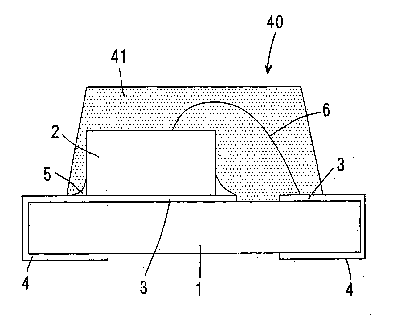
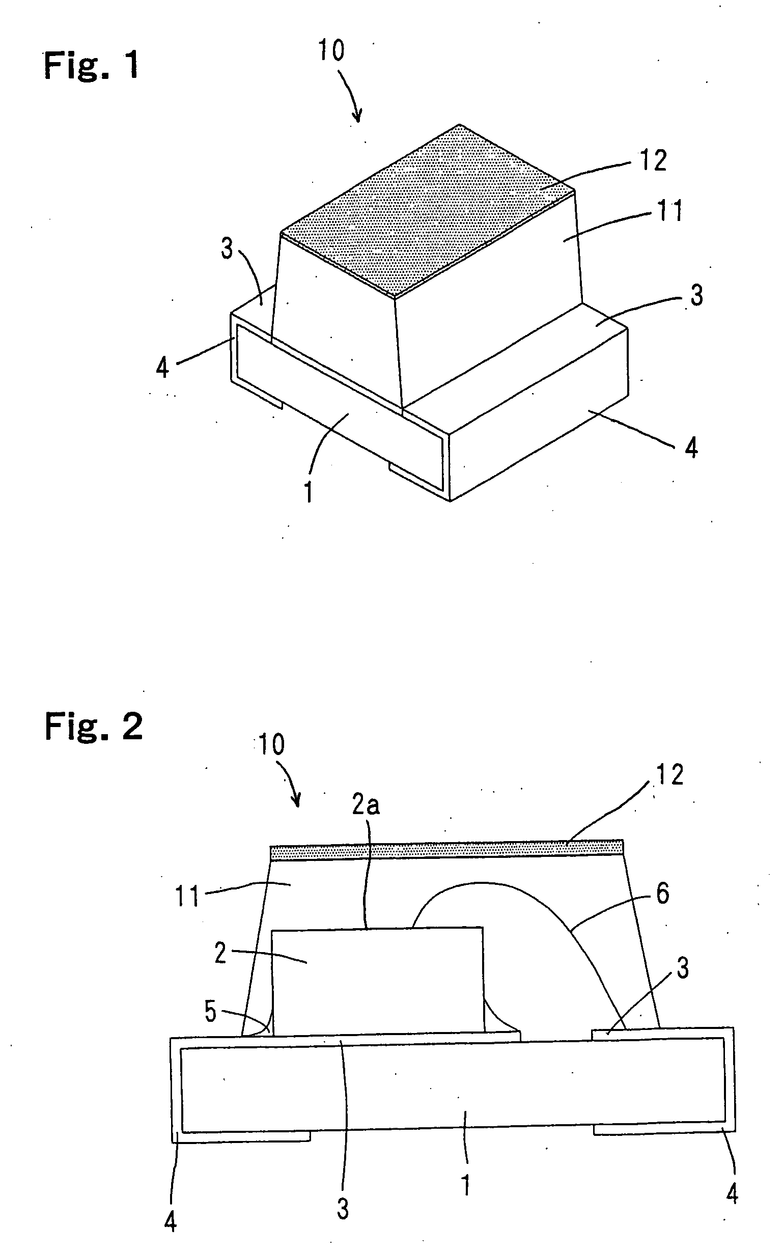
[0063]FIG. 1 is a perspective view showing an optical sensor according to Embodiment 1 of the present invention; and FIG. 2 is a front view in section showing the optical sensor according to Embodiment 1.

[0064] An optical sensor 10 according to Embodiment 1 includes: a substrate 1 having, on a mounting surface thereof, a pair of electrodes (metal pad portions) 3 of opposite polarity; a photodetector 2 electrically connected to the electrodes 3 on the substrate 1; and a light-transmissive resin encapsulating portion 11 for encapsulating the photodetector 2 on the substrate 1; and an infrared-absorbing layer 12 formed on an outer surface of the light-transmissive resin encapsulating portion 11, the infrared-absorbing layer 12 serving as an infrared-blocking layer that is.

[0065] The substrate 1 is made of, for example, glass or an epoxy resin, and shaped in a rectangular plate. The pair of electrodes 3,3 are of opposite polarity and formed at the opposite sides on a moun...

Example

EMBODIMENT 2

[0084]FIG. 9 is a perspective view of an optical sensor according to Embodiment 2 of the present invention; and FIG. 10 is a front view in section showing the optical sensor according to Embodiment 2.

[0085] In an optical sensor 20 according to Embodiment 2, a light-transmissive resin encapsulating portion 21 has an inner resin portion 22 and an outer resin portion 23, the inner resin portion 22 encapsulating the photodetector 2, the outer resin portion 23 covering the inner resin portion 22. The infrared-absorbing layer 12 is made of an infrared-absorbing film interposed between the inner resin portion 22 and the outer resin portion 23. Like reference numerals denote like parts in Embodiment 1 and explanations thereon are omitted.

[0086] The inner resin portion 22 is made of, for example, an epoxy resin having insulating, light-transmissive and thermosetting properties. The outer resin portion 23 is made of, for example, an epoxy resin having light-transmissive and the...

Example

EMBODIMENT 3

[0090] FIGS. 12 are a flowchart showing the step of forming the resin encapsulating portions in the production of an optical sensor according to Embodiment 3 of the present invention.

[0091] In the optical sensor according to Embodiment 3, a transparent adhesive layer 24 is interposed between the transparent resin encapsulating portion 21 and the infrared-absorbing layer 12, of Embodiment 2. A process of producing the optical sensor according to Embodiment 3 will be explained as follows. In the step of forming the resin encapsulating portion, the substrate 1 on which as shown in FIG. 12(a), the inner resin portions 22 are mounted to cover the plurality of photodetectors 2, respectively, is set in the lower mold 91, as shown in FIG. 12(b). Next, a transparent-adhesive-layer formation film 24′ having heat resistance is placed on the inner resin portions 22 on the substrate 1, then the infrared-absorbing-layer formation film 12′ is placed on the transparent-adhesive-layer ...


PUM


Abstract

It is an object of the present invention to provide a highly reliable optical sensor and a production process of the same, the optical sensor being excellent in the characteristic of blocking infrared radiation and capable of being manufactured at a low cost without an increase in the number of steps carried out in the assembly of electronic apparatus. The present invention includes: a substrate 1 having an electrode 3; a photodetector 2 electrically connected to the electrode 3; and a light-transmissive resin encapsulating portion 11 for encapsulating the photodetector 2 on the substrate 1, the optical sensor further including an infrared-blocking layer either inside the light-transmissive resin encapsulating portion 11 or on an outer surface of the light-transmissive resin encapsulating portion 11 for blocking infrared radiation from the outside from reaching the photodetector.

Description

TECHNICAL FIELD [0001] The present invention relates to an optical sensor and a process of producing the same. More particularly, the present invention relates to a surface-mount-type optical sensor to be used for the switching between on and off or adjustment of a light amount of a backlight of a liquid crystal display such as a personal digital assistant and to a process of producing the optical sensor. BACKGROUND ART [0002] In recent years, a rapidly growing number of personal digital assistants including a mobile telephone have employed a TFT color liquid crystal display in their display section, and their power consumption has been rising accordingly. For the purpose of adding the function of turning off or down a backlight source when backlight is not needed (outdoors on a sunny day or indoors with bright illumination), surface-mount-type optical sensors having peak sensitivities at infrared wavelengths have commonly been employed as a component for detecting indoor or outdoor...

Claims


Application Information

Patent Timeline
IPC IPC(8): B29D11/00H01L31/00C09K3/00H01L27/146H01L31/0203H01L31/0216
CPCH01L27/14618H01L31/0203H01L31/02162H01L24/97H01L2224/32225H01L2224/48091H01L2224/97H01L2224/73265H01L2224/48227H01L2924/3025H01L2924/00014H01L2924/00H01L2924/12036H01L2924/12043H01L2924/181H01L31/09
Inventor KAMOSHITA, SHOICHI
Owner SHARP KK
Why Eureka
Try Eureka