Structure and process of embedded chip package

a technology of embedded chips and packaging, applied in the field of embedded chip package structure and process, can solve the problems of unfavorable further use of all other chips, and the manufacturing cost of multi-chip packages is subject to the yield of multi-chip packages

Inactive Publication Date: 2010-01-14
ADVANCED SEMICON ENG INC
View PDF90 Cites 128 Cited by
  • Summary
  • Abstract
  • Description
  • Claims
  • Application Information

AI Technical Summary

Benefits of technology

[0012]In order to make the above and other features and advantages of the present invention more comprehensible, an embodiment accompanied with figures is described in detail below.

Problems solved by technology

Nonetheless, once one of the chips in the multi-chip package is damaged, it is unlikely to further use all of the other chips.
Namely, manufacturing costs of the multi-chip package are subject to yield of the multi-chip package.

Method used


Image

  • Structure and process of embedded chip package
  • Structure and process of embedded chip package
  • Structure and process of embedded chip package

Examples


Embodiment Construction

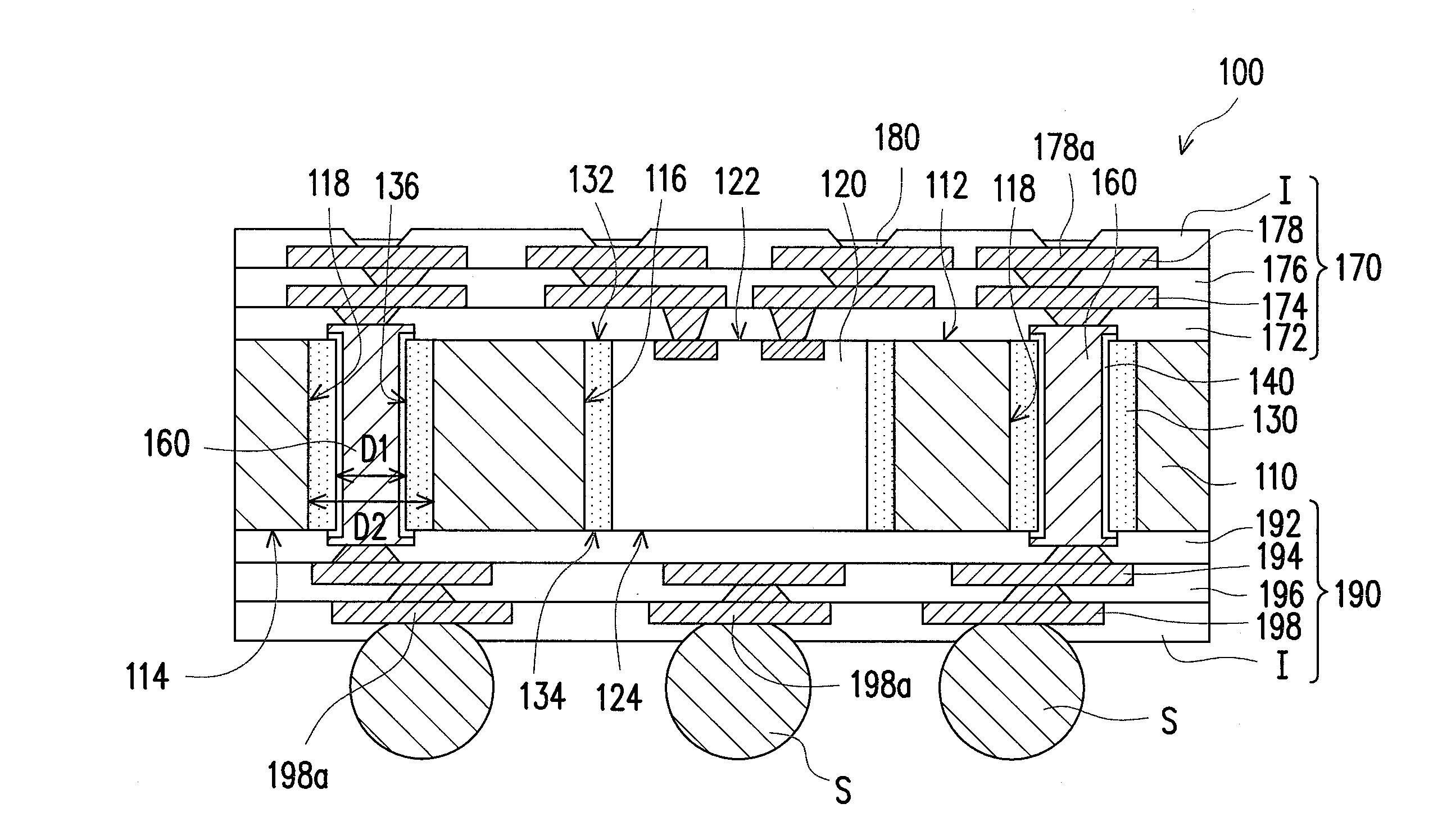
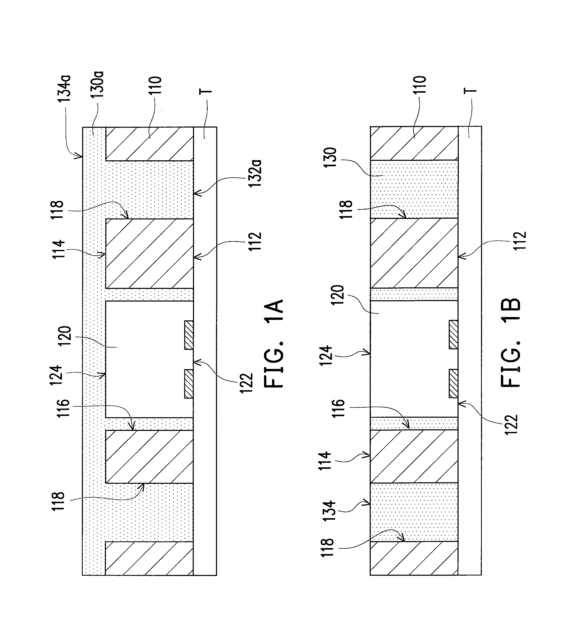
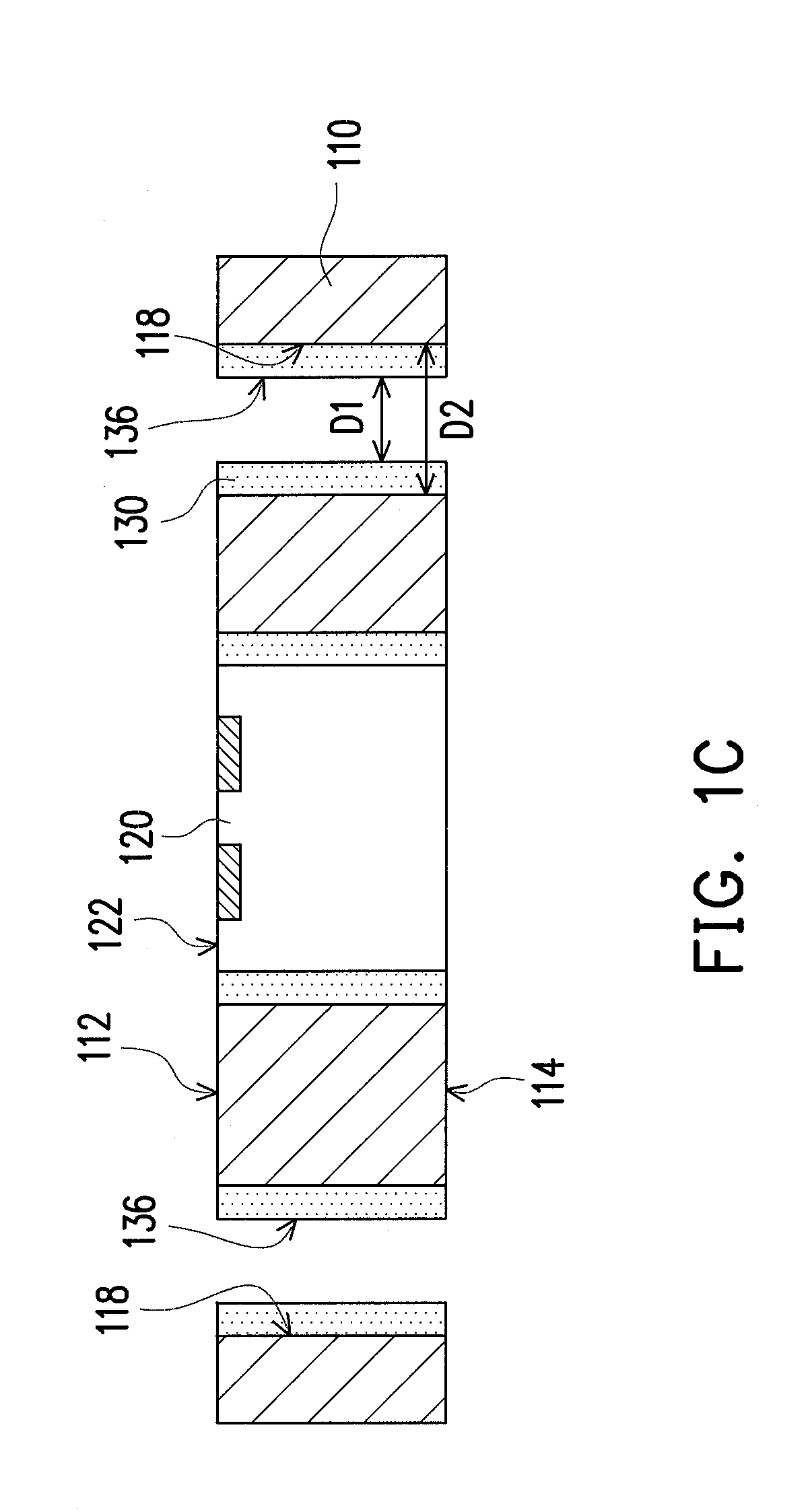
[0015]FIGS. 1A through 1O are schematic cross-sectional views illustrating a process of an embedded chip package according to an embodiment of the present invention.

[0016]Firstly, referring to FIG. 1A, a metal core layer 110 having a first surface 112, a second surface 114 opposite to the first surface 112, an opening 116, and a plurality of first through holes 118 are provided. The opening 116 and the first through holes 118 penetrate the metal core layer 110 and connect the first surface 112 and the second surface 114. As indicated in FIG. 1A, a thermal release material T is then adhered to the first surface 112 of the metal core layer 110. Besides, the thermal release material T covers the first through holes 118 and the opening 116.

[0017]Note that the metal core layer 110 is substantially shaped as a round plate (similar to a wafer shape) in the present embodiment. Hence, the process described in the present embodiment can be performed on the metal core layer 110 with use of sem...


PUM

PropertyMeasurementUnit
diametersaaaaaaaaaa
thermal releaseaaaaaaaaaa
dielectricaaaaaaaaaa

Abstract

A process of an embedded chip package structure includes following steps. Firstly, a metal core layer having a first surface, a second surface opposite to the first surface, an opening, and a number of through holes are provided. The opening and the through holes connect the first surface and the second surface. A chip is then disposed in the opening. Next, a dielectric layer is formed in the opening and the through holes to fix the chip in the opening. Thereafter, a number of conductive vias are respectively formed in the through holes and insulated from the metal core layer by a portion of the dielectric layer located in the through holes. A circuit structure is then formed on the first surface of the metal core layer by performing a build-up process, and the circuit structure electrically connects the chip and the conductive vias.

Description

CROSS-REFERENCE TO RELATED APPLICATION[0001]This application claims the priority benefit of Taiwan application serial no. 97143131, filed on Nov. 7, 2008. The entirety of the above-mentioned patent application is hereby incorporated by reference herein and made a part of specification.BACKGROUND OF THE INVENTION[0002]1. Field of the Invention[0003]The present invention relates to a chip package technology, and more particularly to an embedded chip package structure and a process of an embedded chip package.[0004]2. Description of Related Art[0005]A chip package aims at providing proper signal transmission paths and heat dissipation paths as well as protecting the chip structure. A leadframe serving as a carrier of a chip is frequently employed in a conventional wire bonding technique. As contact density in a chip gradually increases, the leadframe which is unable to satisfy current demands on the high contact density is replaced by a package substrate which can achieve favorable con...

Claims


Application Information

Patent Timeline
Patent Type & Authority Applications(United States)
IPC IPC(8): H05K1/16H05K13/00
CPCH01L21/486Y10T29/49172H01L23/49816H01L23/49822H01L23/49827H01L23/5389H01L24/19H01L25/105H01L2221/68345H01L2221/68359H01L2224/04105H01L2224/20H01L2924/01029H01L2924/01046H01L2924/01078H01L2924/01079H01L2924/15311H01L2924/15331H01L2924/18162H05K1/056H05K1/185H05K3/445H05K3/4608H05K2201/09536H05K2201/10674H01L2924/01005H01L2924/01033H01L21/6835
Inventor FU, CHIEH-CHENOU, YING-TEWANG, YUNG-HUI
Owner ADVANCED SEMICON ENG INC
Why Eureka
Try Eureka