
Model Based Hint Generation For Lithographic Friendly Design

a technology of lithographic friendly design and model, applied in the field of integrated circuit design and manufacturing, can solve the problems of defect change, reduced feature size, and difficult stabilization of manufacturing yields,

Inactive Publication Date: 2010-01-28
CHEW MARKO P +2
View PDF13 Cites 22 Cited by
  • Summary
  • Abstract
  • Description
  • Claims
  • Application Information

AI Technical Summary

Problems solved by technology

This reduction in feature size increases the difficulty of faithfully reproducing the image intended by the layout design onto the substrate.
Additionally, manufacturing yields are difficult to stabilize even after manufacturing processes have been refined.
A principal reason for declining yields is that as feature sizes shrink, the dominant cause of defects change.
At larger process technologies, yield limitation is dominated by random defects.
Despite the best clean room efforts, particles still find a way to land on chips or masks, causing shorts or opens.
In smaller process technologies, for example the nanometer process technology, the dominant source of yield loss is pattern-dependent effects.
These defects are a result of the design's features being smaller than the wavelength of light.
Although these extensive modifications to the physical layout design resulted in a layout design that was unrecognizable by the designer, the resulting manufactured circuit matched the designer's intent.
As indicated above, designs and the optical lithographic processes used to manufacture the designs are increasing in complexity.
Accordingly, generation of optical models as well as application of resolution enhancement techniques such as optical proximity correction is increasingly burdensome.

Method used


Image

  • Model Based Hint Generation For Lithographic Friendly Design
  • Model Based Hint Generation For Lithographic Friendly Design
  • Model Based Hint Generation For Lithographic Friendly Design

Examples


Embodiment Construction

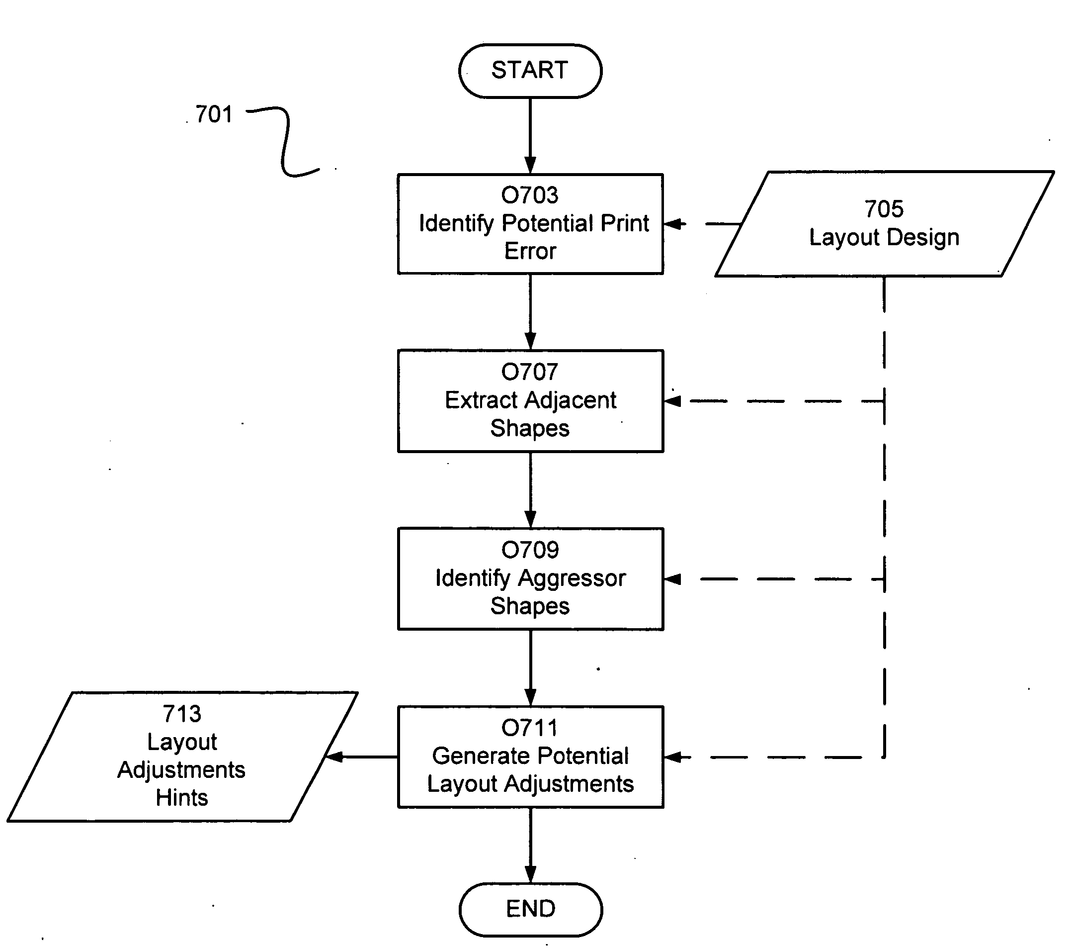
[0034]Although the operations of the disclosed methods are described in a particular sequential order for convenient presentation, it should be understood that this manner of description encompasses rearrangements, unless a particular ordering is required by specific language set forth below. For example, operations described sequentially may in some cases be rearranged or performed concurrently. Moreover, for the sake of simplicity, the disclosed flow charts and block diagrams typically do not show the various ways in which particular methods can be used in conjunction with other methods. Additionally, the detailed description sometimes uses terms like “determine” to describe the disclosed methods. Such terms are high-level abstractions of the actual operations that are performed. The actual operations that correspond to these terms will vary depending on the particular implementation and are readily discernible by one of ordinary skill in the art.

[0035]Some of the methods describe...


PUM


Abstract

In various implementations of the invention, a model of an optical proximity correction process is employed to determine potential adjustments to a layout design for a mask that might resolve potential errors an image resulting from application of the mask in an optical lithographic process. In various implementations of the invention, corrected mask shapes, such as for example optical proximity corrected mask shapes, and associated printed image contours are generated through use of a model. Subsequently, the associated printed image contour and a desired printed image contour may be used to determine various edge segment adjustments to the corrected mask shapes that would realize the desired printed image contour. In various implementations of the present invention, the model for generation of the corrected mask shapes and the associated printed image contour is a square kernel model. With various implementations of the invention, the kernel represents a grey scale map wherein each pixel of the map is generated based on the desired displacement relative to the displacement to be modeled. For example by application of linear regression techniques. As a result, printed image contours and corrected mask shapes may be generated based upon an input layout design, wherein potential adjustments to the mask may be determined based upon a desired printed image contour.

Description

RELATED APPLICATIONS[0001]This application claims priority under 35 U.S.C. §119 to and is a continuation of U.S. patent application Ser. No. 12 / 184,089, entitled “Model Based Microdevice Design Layout Correction,” filed on Jul. 31, 2008, and naming Marko Chew et al. as inventors, which application claims priority to U.S. Provisional Patent Application No. 60 / 962,814 entitled “FPOPC-Based Hint Generation for LFD Integration to P&R,” filed on Jul. 31, 2007, and naming Marco Chew et al. as inventors. This application further claims priority to U.S. Provisional Patent Application No. 61 / 040,873, entitled “Square Kernel Lithographic Friendly Design Models,” filed on Mar. 31, 2008 and naming Yuri Granik et al. as inventors. The above referenced applications are all incorporated entirely herein by reference.FIELD OF THE INVENTION[0002]The invention relates to the field of integrated circuit design and manufacturing. More particularly, various implementations of the invention are applicable...

Claims


Application Information

Patent Timeline
Patent Type & Authority Applications(United States)
IPC IPC(8): G06F17/50
CPCG06F2217/12G06F17/5081G06F30/398G06F2119/18Y02P90/02
Inventor CHEW, MARKO P.YANG, YUETORRES ROBLES, JUAN ANDRES
Owner CHEW MARKO P
Learn More