Semiconductor device having recess gate and isolation structure and method for fabricating the same

a technology of isolation structure and semiconductor device, which is applied in the direction of semiconductor device, basic electric element, electrical apparatus, etc., can solve the problems of reducing the rule, affecting the operation of the transistor, and limiting the process of filling the trench by a high density plasma process, so as to reduce the operation. the effect of the transistor operation

Inactive Publication Date: 2010-04-01
SK HYNIX INC
View PDF6 Cites 35 Cited by
  • Summary
  • Abstract
  • Description
  • Claims
  • Application Information

AI Technical Summary

Benefits of technology

[0031]According to the embodiments of the invention, a semiconductor device having a recess gate and an isolation structure, which can restrict lowering of operation properties of a transistor due to a tensile stress caused by a SOD when forming a STI structure using a SOD, and a method for fabricating the same can be provided.

Problems solved by technology

As the design rule is sharply reduced, a process of filling the trench by a High Density Plasma process has shown a limitation.
Spreading of the stress caused from the SOD to the bottom corner of the recess groove can result in a partial concentration of voltage to the bottom corner of the recess groove during operation of the transistor.

Method used


Image

  • Semiconductor device having recess gate and isolation structure and method for fabricating the same
  • Semiconductor device having recess gate and isolation structure and method for fabricating the same
  • Semiconductor device having recess gate and isolation structure and method for fabricating the same

Examples


Embodiment Construction

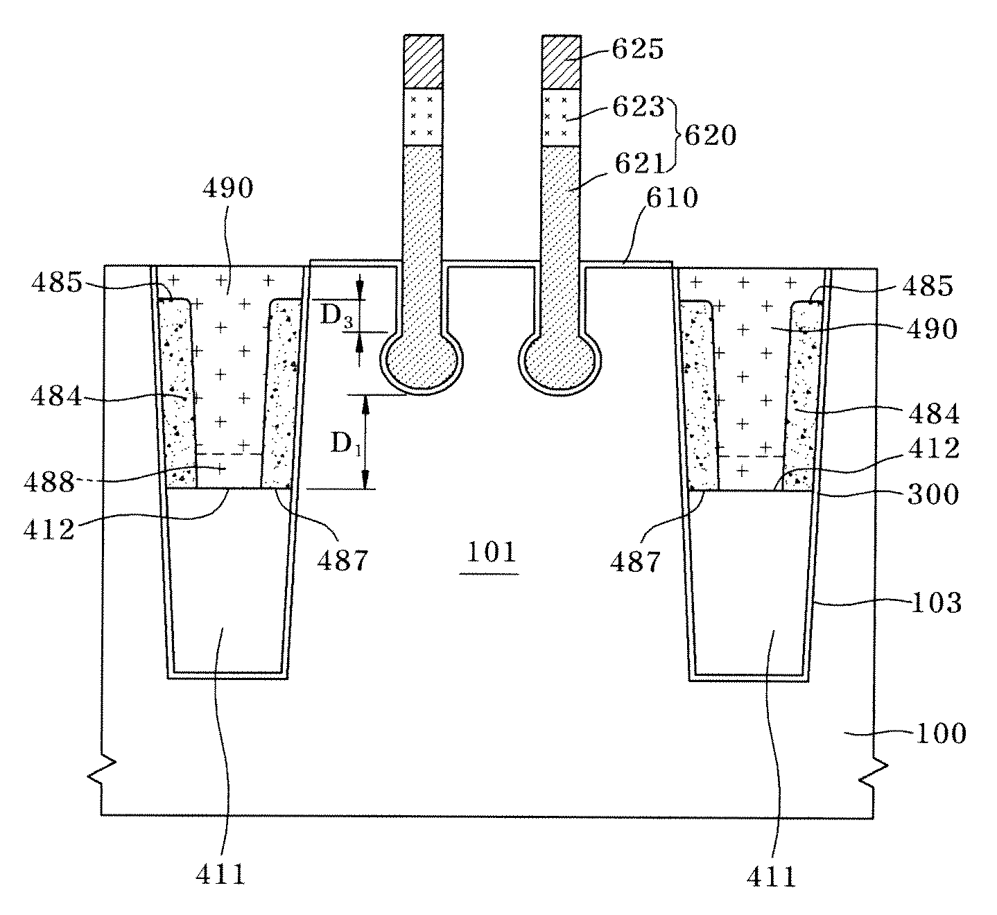
[0036]Embodiments of the invention are directed to a semiconductor that can prevent the lowering of the operation properties of a transistor including a recess gate by a tensile stress caused by a SOD layer during formation of a STI structure using the SOD. The semiconductor includes an isolation structure having a HDP oxide layer disposed in a portion of the isolation trench corresponding to the bottom of a recess groove, and SOD layers disposed at the upper and lower sides of the HDP oxide layer to fill the isolation trench.

[0037]The HDP oxide layer is relatively denser than the SOD layer, thus making it difficult for a stress to be generated and spread. The HDP oxide layer is disposed in the portion of the isolation trench corresponding to the bottom of the recess groove, making it possible to effectively restrict the tensile stress caused by the SOD from having a direct influence on the recess groove. Therefore, it is possible to effectively restrict degradation of operation pro...


PUM


Abstract

Disclosed herein is a semiconductor device including an isolation structure and a recess gate and a method for fabricating the same. The method for fabricating a semiconductor device includes: forming a trench by selectively etching an isolation region of a semiconductor substrate to define an active region; forming a first SOD partially filling the trench; forming a stress shielding layer, which is denser than the first SOD, over the first SOD; forming a second SOD that fills the trench over the first SOD including the stress shielding layer; forming a recess groove by selectively etching a portion of the active region, wherein an upper surface of the first SOD is spaced downwardly from a bottom of the recess groove, and an upper surface of the stress shielding layer is spaced upwardly from the bottom of the recessed groove; and forming a gate of a transistor that fills the recess groove.

Description

CROSS-REFERENCE TO RELATED APPLICATION[0001]Priority to Korean patent application No. 10-2008-0095555, filed on Sep. 29, 2008, the disclosure of which is incorporated herein by reference in its entirety, is claimed.BACKGROUND OF THE INVENTION[0002]The invention relates to a semiconductor device, and more particularly, to a semiconductor device structure including an isolation structure and a recess gate and a method for fabricating the same.[0003]With increased integration of semiconductor memory devices, a design rule of circuit patterns is sharply reduced. For example, as a design rule of a Dynamic Random Access Memory (DRAM) device is reduced to less than about 50 nm, formation of finer patterns is required. Such reduction in the design rule requires superior gap fill properties in a process of forming an isolation structure. In formation of the isolation structure by a Shallow Trench Isolation (STI) method, a sharp increase in an aspect ratio of the trench and a decrease in a wi...

Claims


Application Information

Patent Timeline
Patent Type & Authority Applications(United States)
IPC IPC(8): H01L29/06H01L21/762
CPCH01L21/76232H01L29/66621H01L27/10876H10B12/053H01L21/18H01L21/76
Inventor EUN, BYUNG SOO
Owner SK HYNIX INC
Why Eureka
Try Eureka