

Patterning method
- Summary
- Abstract
- Description
- Claims
- Application Information
AI Technical Summary
Benefits of technology
Problems solved by technology
Method used
Image

Examples
first embodiment
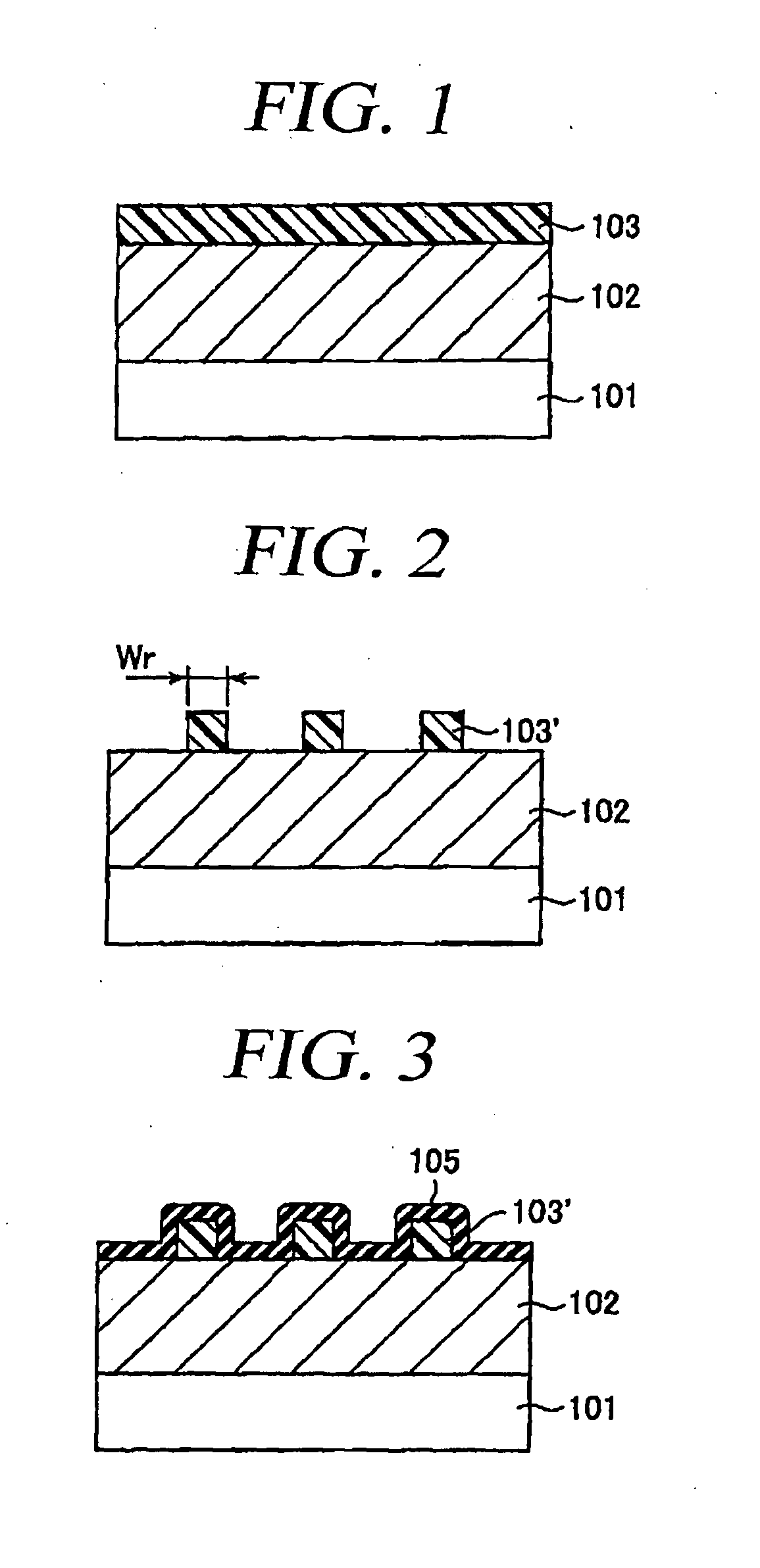
[0051]FIGS. 1 to 6 provide cross sectional views to illustrate every major manufacturing process of a patterning method in accordance with a first embodiment of the present invention.
[0052]The first embodiment illustrates a basic processing sequence of the patterning method in accordance with the present invention.
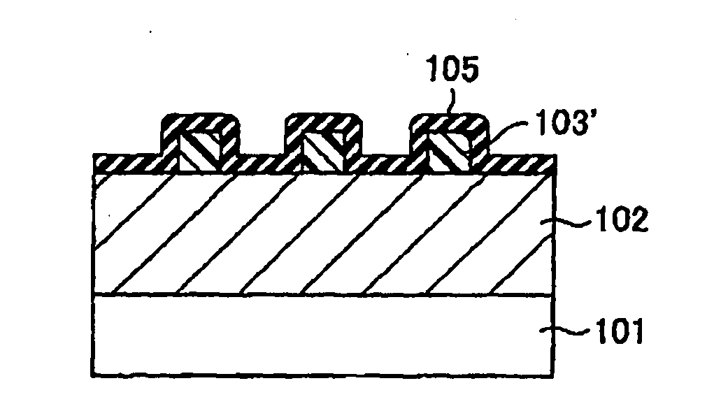
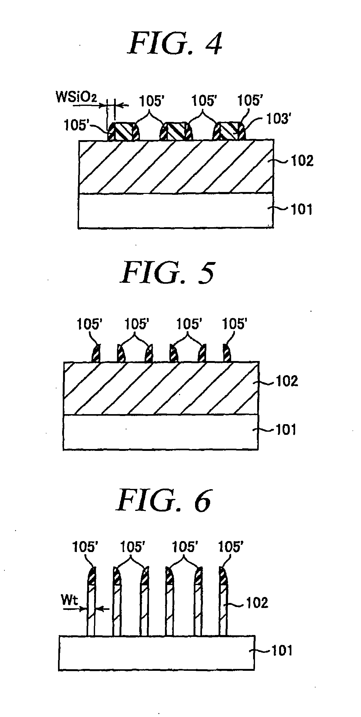
[0053]First, as shown in FIG. 1, a thin film 102 is formed on a semiconductor substrate 101. In the present specification, the semiconductor substrate 101 does not merely imply a semiconductor substrate, e.g., a silicon substrate, but includes a structure body having, in or on the semiconductor substrate, a semiconductor device, a conductive film corresponding to an integrated circuit pattern and an interlayer insulating film which insulates them. The thin film 102 is processed into a micro pattern later. The thin film 102 may be an insulating film different from a sidewall spacer to be formed later, or may be a conductive film. In the present embodiment, the thin film 102...
second embodiment
[0112]FIGS. 12 to 18 provide cross sectional views to describe every major manufacturing process of a patterning method in accordance with a second embodiment of the present invention.
[0113]The second embodiment illustrates an example of the patterning method in accordance with the present invention, which can be more desirably applied to an actual semiconductor manufacturing process.
[0114]First, as shown in FIG. 12, an etching stopper film 106 is formed on a semiconductor substrate 101. The etching stopper film 106 functions to stop etching when a thin film to be formed on top of it is etched. In the present embodiment, the etching stopper film 106 is, e.g., a silicon nitride film. Subsequently, a thin film 102 formed of a different material from the etching stopper film 106 is formed on the etching stopper film 106. In the present embodiment, the thin film 102 is, e.g., a conductive polysilicon film, as in the first embodiment. Subsequently, a hard mask film 107 made of a differen...
third embodiment
[0125]FIGS. 19 to 24 present cross sectional views to illustrate every major manufacturing process of a patterning method in accordance with a third embodiment of the present invention.
[0126]The third embodiment provides an example of trimming a resist pattern 103′. By trimming the resist pattern 103′, finer micro patterns made of a thin film 102 can be formed.
[0127]First, as shown in FIG. 19, the resist pattern 103′ is formed on the thin film 102 according to the method described with reference to FIGS. 1 and 2. In the present embodiment, a width Wr of the resist pattern 103′ in the plane direction is set to be approximately equal to a resolution limit.
[0128]Subsequently, as illustrated in FIG. 20, the resist pattern 103′ is trimmed, so that a trimmed resist pattern 103′S is obtained (referred to as “trimming process” in the present specification). The trimming process is performed at a temperature ranging from a room temperature to about 100° C. under the atmosphere containing oxy...
PUM
 Abstract
Description
Claims
Application Information