Automatic word line leakage measurement circuitry

Active Publication Date: 2010-05-20
MICRON TECH INC
View PDF48 Cites 21 Cited by
  • Summary
  • Abstract
  • Description
  • Claims
  • Application Information

AI Technical Summary

Problems solved by technology

The continued down scaling of MOS devices has created many challenges and opportunities, among them the formidable requirement for an ultra-thin gate oxide.
One serious problem that comes along with thin oxide, and hinders further down scaling, is excessive leakage current.
Since the excessive leakage current for such an ultra-thin oxide will be unacceptable for very-large-scale integration (VLSI) applications, it is imperative that flash memories with unacceptable leakage current be identified during manufacturing process.
However, this kind of leakage measurement takes longer time than ideal since leakage current is measured from outside of the memory devices.
This results in long test time and leads to long manufacturing cycle, which translates into high cost of production.

Method used


Image

  • Automatic word line leakage measurement circuitry
  • Automatic word line leakage measurement circuitry
  • Automatic word line leakage measurement circuitry

Examples


Embodiment Construction

[0016]Described herein is a memory device and method for measuring leakage on the plurality of word lines in a memory device. The following description sets forth numerous specific details such as examples of specific systems, components, methods, and so forth, in order to provide a good understanding of several embodiments of the present invention. It will be apparent to one skilled in the art, however, that at least some embodiments of the present invention may be practiced without these specific details. In other instances, well-known components or methods are not described in detail or are presented in simple block diagram form in order to avoid unnecessarily obscuring the present invention. Thus, the specific details set forth are merely for illustration purpose. Particular implementations may vary from these illustration details and still be contemplated to be within the spirit and scope of the present invention.

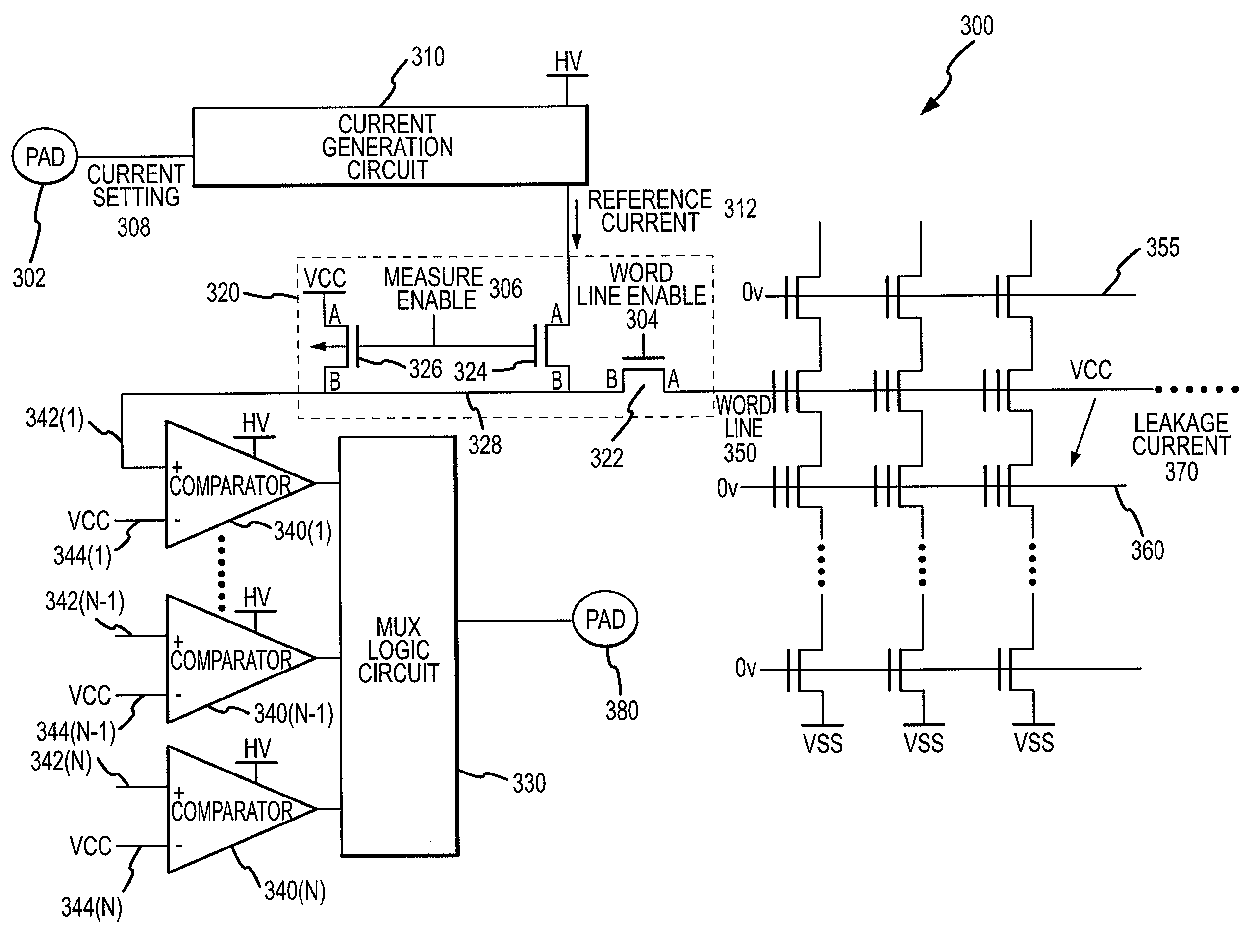
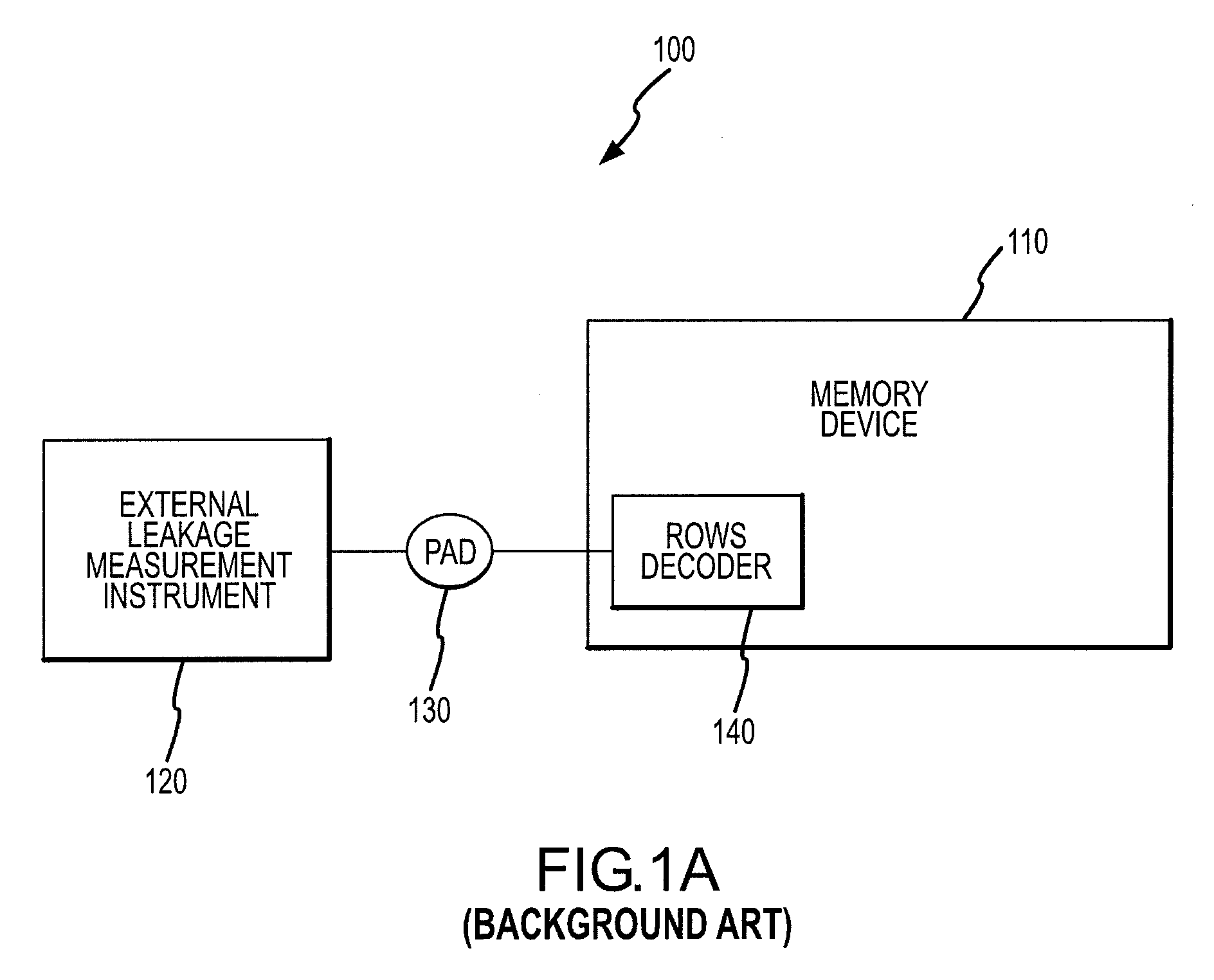
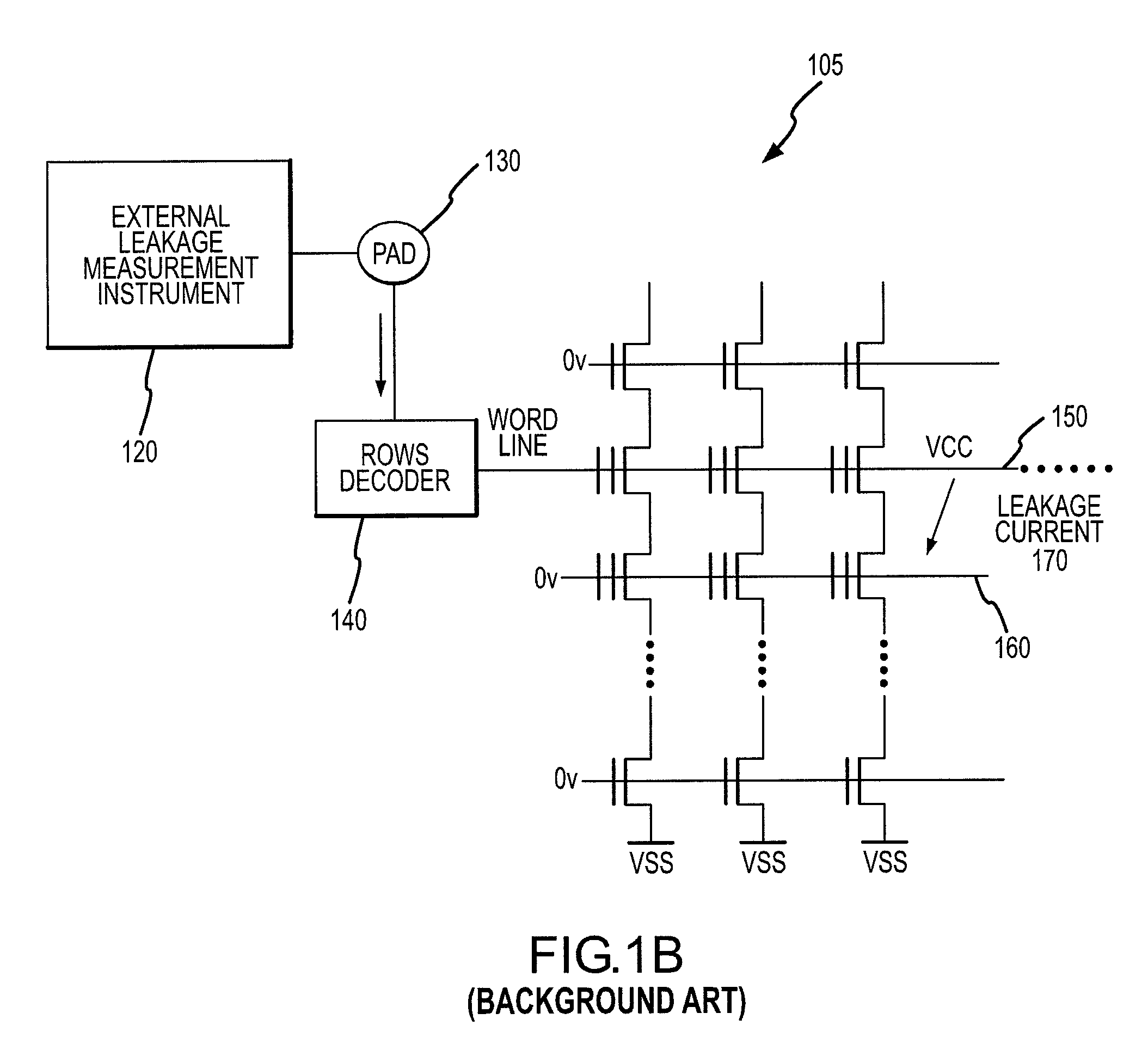
[0017]A leakage measurement system 200 according to one embodimen...


PUM


Abstract

The present invention is a circuit and method for measuring leakage on the plurality of word lines in a memory device. In one embodiment, a memory device may include a leakage measurement circuit that is coupled to a plurality of word lines of the memory device. The leakage measurement circuit may be operable to generate a reference current and to determine whether a leakage current on one of the plurality of word lines is acceptable relative to the reference current. In another embodiment, a method may include determining whether leakage on one of a plurality of word lines of a memory device is allowable using a circuit in the memory device.

Description

TECHNICAL FIELD[0001]This invention relates generally to memory devices, and more particularly, to leakage measurement in a memory device.BACKGROUND OF THE INVENTION[0002]With increasing popularity of electronic devices, such as laptop computers, portable digital assistants, digital cameras, mobile phones, digital audio players, video game consoles and the like, demand for nonvolatile memories are on the rise. Nonvolatile memories come in various types, including flash memories. Flash memories are widely used nowadays for fast information storage in electronic devices such as those mentioned above.[0003]In flash memories, data bits are stored in an array of individual memory cells, each of which includes a floating gate transistor. Generally speaking, each of the memory cells in a flash memory looks similar to a standard metal-oxide-semiconductor field-effect transistor (MOSFET), except that a flash memory cell has two gates instead of just one. One gate, the control gate, is analog...

Claims


Application Information

Patent Timeline
IPC IPC(8): G01R19/00G11C16/06G11C5/14G11C7/00
CPCG11C16/04G11C29/02G11C2029/5006G11C2029/1202G11C29/025G11C7/1006G11C7/062G11C16/08
Inventor YAMADA, SHIGEKAZU
Owner MICRON TECH INC
Why Eureka
Try Eureka