
Pixel structure

a technology of pixel structure and pixel structure, which is applied in the direction of diodes, semiconductor devices, instruments, etc., can solve the problems of color shift problems already facing a technology bottleneck, difficulty in purchasing white light-emitting diodes that meet the above-mentioned requirements, and relatively high cost and technical difficulties

Active Publication Date: 2010-05-27
AU OPTRONICS CORP
View PDF6 Cites 16 Cited by
  • Summary
  • Abstract
  • Description
  • Claims
  • Application Information

AI Technical Summary

Benefits of technology

[0011]The present invention provides a pixel structure which provides a correct white balance.
[0024]The present invention uses the second white light provided by the white sub-pixel to obtain the required white balance, and there is no need to adjust the ratio of the areas of the sub-pixel or the spectrum of the backlight module. The present invention therefore has better practicability.

Problems solved by technology

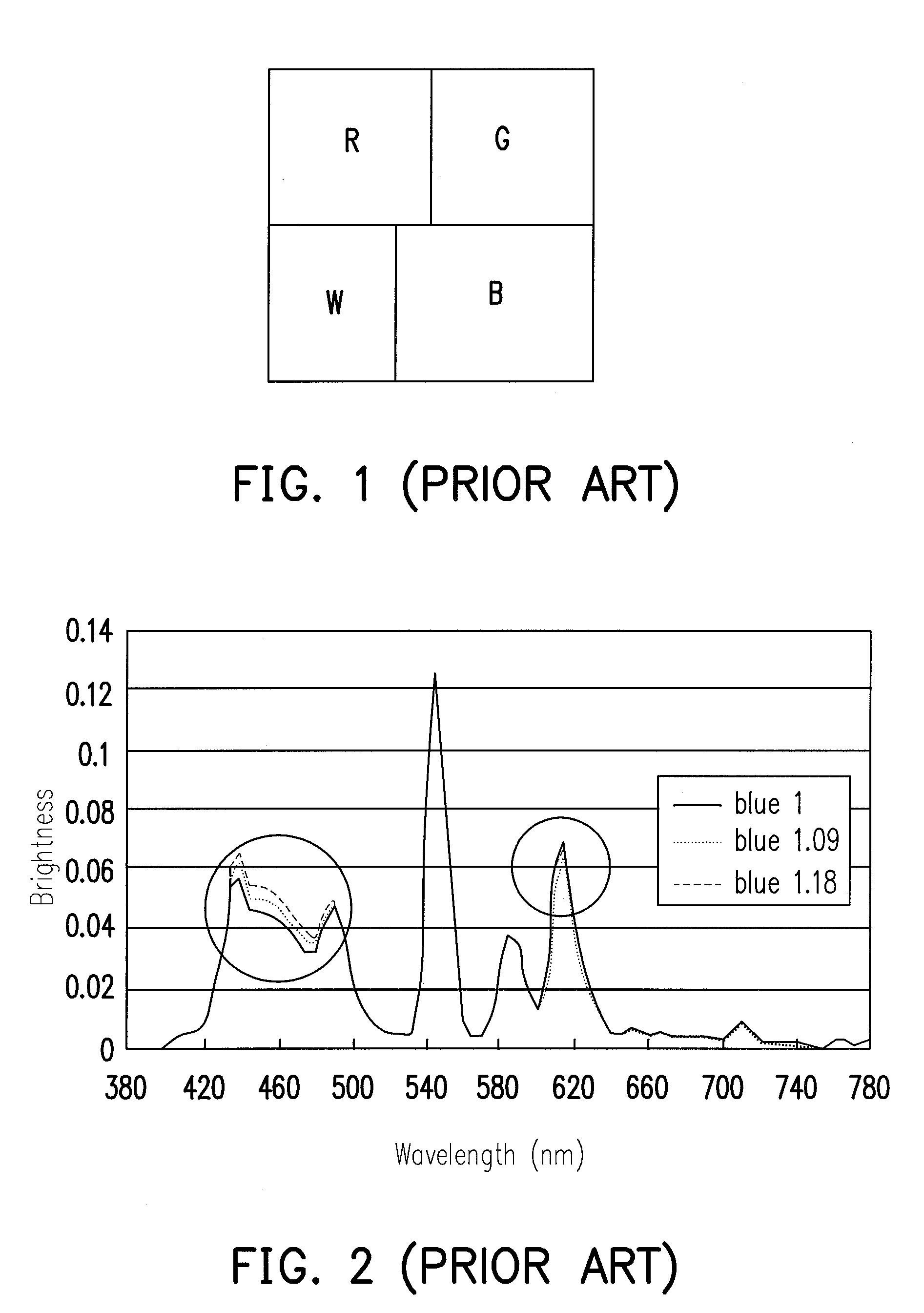
However, as limited by specifications the white light-emitting diodes currently produced, the white light-emitting diode that meets the above-mentioned requirements is difficult to purchase.
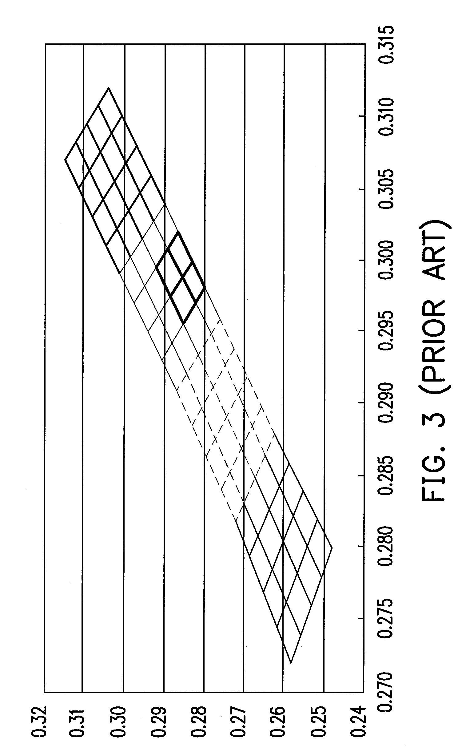
Hence, methods of adjusting the backlight to improve the problems of the color shift are already facing a technological bottleneck.
Accordingly, no matter modifying the ratio of the areas of the pixels or adjusting the spectrum of the backlight module, costs and technical difficulties thereof have relatively increased.

Method used


Image

  • Pixel structure
  • Pixel structure
  • Pixel structure

Examples


Embodiment Construction

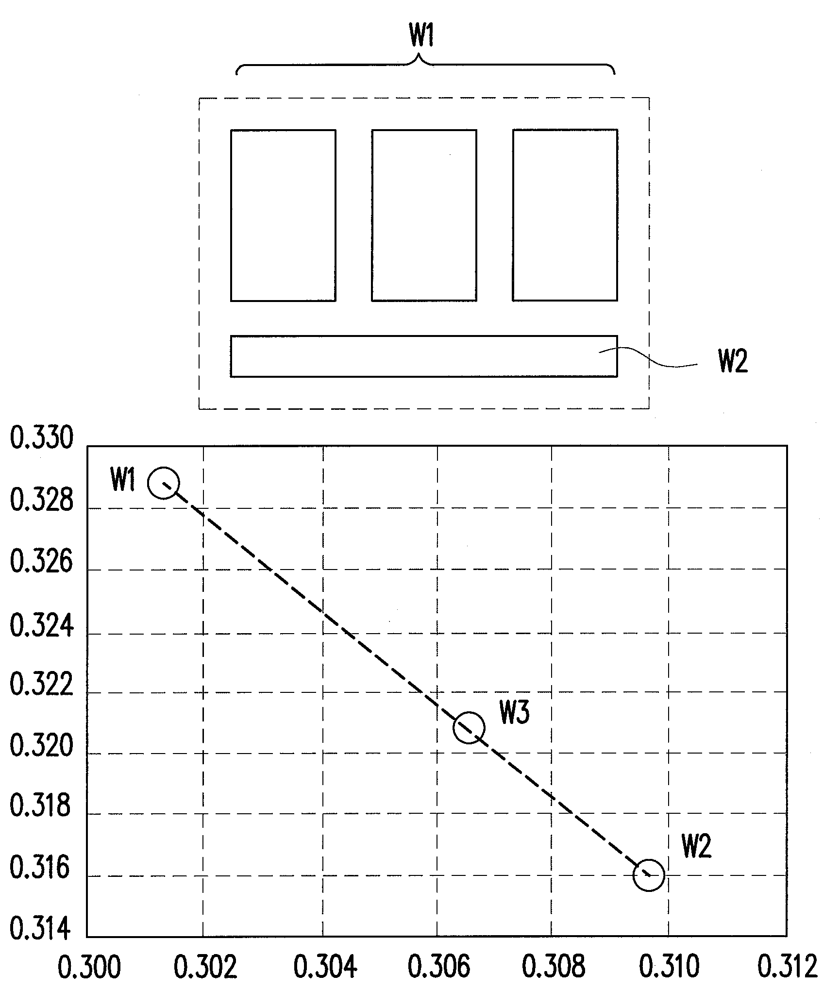
[0035]FIG. 5A is a schematic diagram of a pixel structure according to an embodiment of the present invention. Referring to FIG. 5A, a pixel structure 100 includes a red sub-pixel 110, a green sub-pixel 120, a blue sub-pixel 130 and a white sub-pixel 140, and the red sub-pixel 110, the green sub-pixel 120 and the blue sub-pixel 130 are suitable for providing a first white light W1 having a chroma coordinate (x1, y1), while the white sub-pixel 140 is suitable for providing a second white light having a chroma coordinate (x2, y2), wherein (x1, y1)≠(x2, y2), x2≧x1 and y2≦y1.

[0036]According to the present embodiment, the red sub-pixel 110, the green sub-pixel 120, the blue sub-pixel 130 and the white sub-pixel 140 may be non-self-luminous sub-pixels, for example LCD sub-pixels. By using a backlight module to make the red sub-pixel 110, the green sub-pixel 120 and the blue sub-pixel 130 in the pixel structure 100 display a red light having a chroma coordinate (xR, yR), a green light havi...


PUM

PropertyMeasurementUnit
pixel structureaaaaaaaaaa
brightnessaaaaaaaaaa
weightaaaaaaaaaa

Abstract

A pixel structure includes a red sub-pixel, a green sub-pixel, a blue sub-pixel and a white sub-pixel. The red sub-pixel, the green sub-pixel and the blue sub-pixel are suitable for providing a first white light, and a chroma coordinate of the first white light is (x1, y1). The white sub-pixel is suitable for providing a second white light, and a chroma coordinate of the second white light is (x2, y2). The chroma coordinate of the first white light is different from the chroma coordinate of the second white light, that is, (x1, y1)≠(x2, y2), while x2≧x1 and y2≦y1.

Description

CROSS-REFERENCE TO RELATED APPLICATION[0001]This application claims the priority benefit of Taiwan application serial no. 97145212, filed on Nov. 21, 2008. The entirety of the above-mentioned patent application is hereby incorporated by reference herein and made a part of specification.BACKGROUND OF THE INVENTION[0002]1. Field of the Invention[0003]The present invention relates to a pixel structure, particularly relates to a pixel structure having a red sub-pixel, a green sub-pixel, a blue sub-pixel and a white sub-pixel.[0004]2. Description of Related Art[0005]As technology constantly advances, expectations of display quality of displays by people continuously increase. Not only are images of the displays desired to have high resolutions, high brightness and high contrast, displays are also desired to have advantages of light weight and low energy consumption. In conventional liquid crystal display (LCD) panels, a pixel structure thereof includes a red sub-pixel, a green sub-pixel ...

Claims


Application Information

Patent Timeline
Patent Type & Authority Applications(United States)
IPC IPC(8): G02F1/1335G02F1/13357
CPCG02F2201/52H01L27/3232H01L27/3213H10K59/351H10K59/50
Inventor CHU KE, HUISUN, WEI-CHIEHWANG, CHUN-CHIEHCHENG, SHENG-WEN
Owner AU OPTRONICS CORP
Learn More