Stacked piezoelectric device

a piezoelectric device and piezoelectric technology, applied in the direction of generators/motors, mechanical equipment, machines/engines, etc., can solve the problems of sacrificing the amount of displacement, concentrating stress at the interface, and cracks in the device, so as to avoid the drop in insulation resistance.

Active Publication Date: 2010-06-10
DENSO CORP
View PDF5 Cites 23 Cited by
  • Summary
  • Abstract
  • Description
  • Claims
  • Application Information

AI Technical Summary

Benefits of technology

[0041]Therefore, the piezoelectric ceramic layer including the stress absorbing portion is used as a drive source, but application of an excessive electric field to the stress absorbing portions is controlled or avoided. It is, therefore, possible to avoid the drop in insulation resistance without almost sacrificing the amount of displacement.

Problems solved by technology

However, the formation of the inner electrode-unformed areas in order to improve the insulation may cause portions which are susceptible and insusceptible to deformation to appear in the ceramic laminate upon application of voltage thereto, resulting in concentration of stress at interfaces therebetween and cracks in the device.
However, even when the stress absorbing portions are formed, the application of the voltage to the stress absorbing portions also may result in cracks extending from the top end of the stress absorbing portions.
Such a structure, however, causes great electric discharge to occur at the stress absorbing portions (grooves) upon application of great voltage thereto, so that they may be short-circuited.
This gives rise to the problem of insufficient electric insulation, which results in a decrease in service life of the stacked piezoelectric devices.
However, in fact, even when no cracks occur in the stress absorbing portions, it is still difficult to ensure sufficient electric insulation, which gives rise to the problem of a drop in electric insulation, thus resulting in formation of cracks.
This results in the problem of a decreased amount of stroke of the stacked piezoelectric devices.

Method used


Image

  • Stacked piezoelectric device
  • Stacked piezoelectric device
  • Stacked piezoelectric device

Examples


embodiments

Embodiment 1

[0183]Next, the stacked piezoelectric device according to embodiments of the invention will be described below using FIGS. 1 to 10.

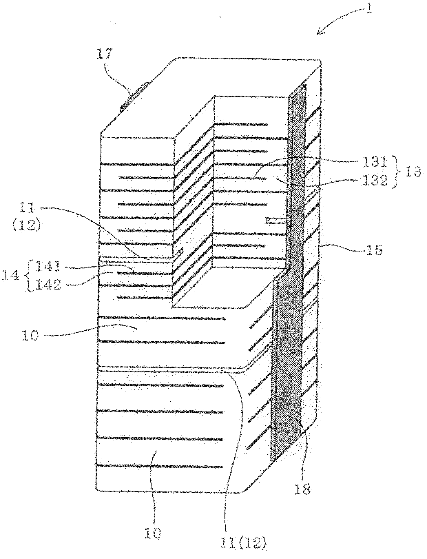
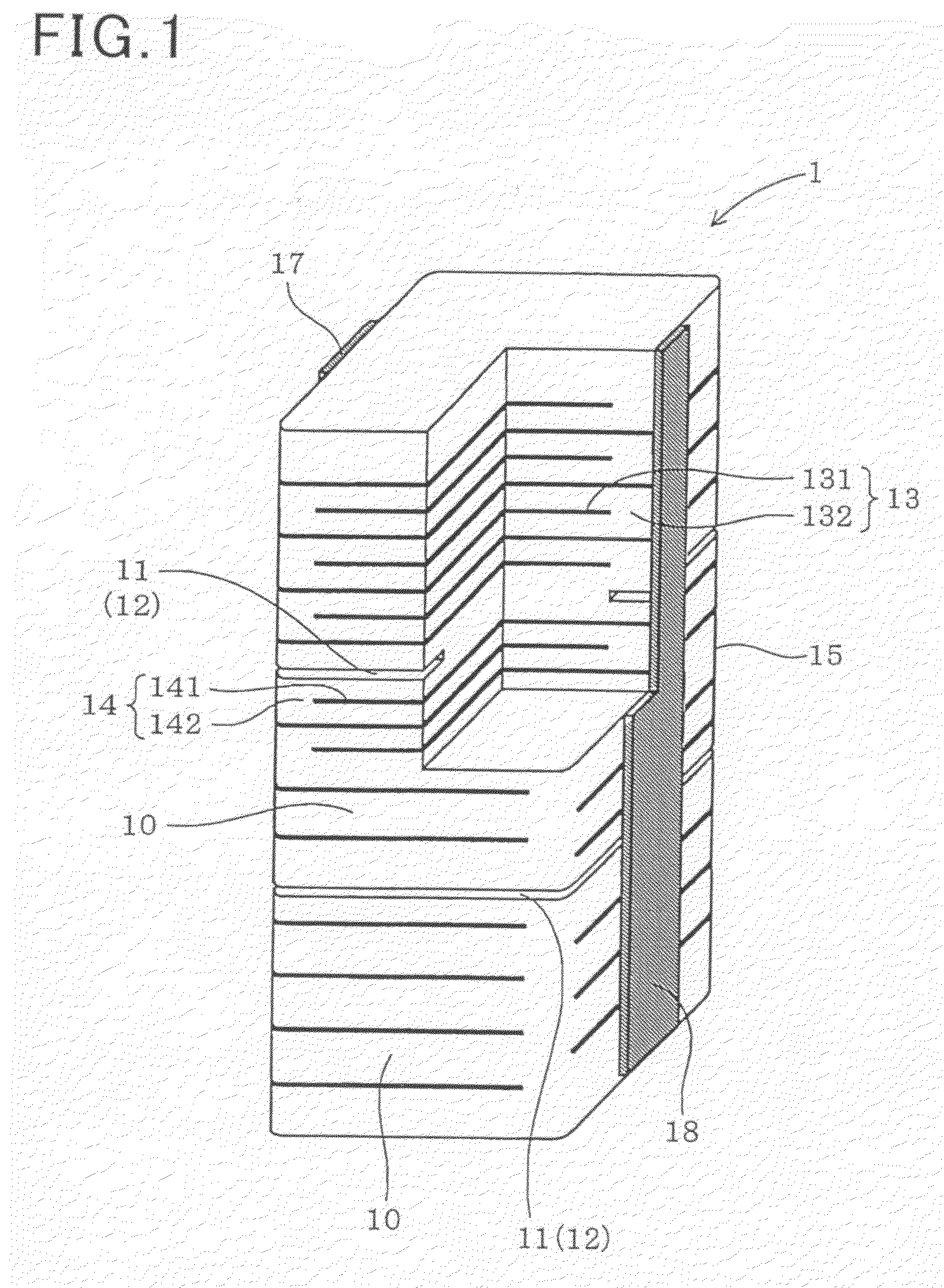
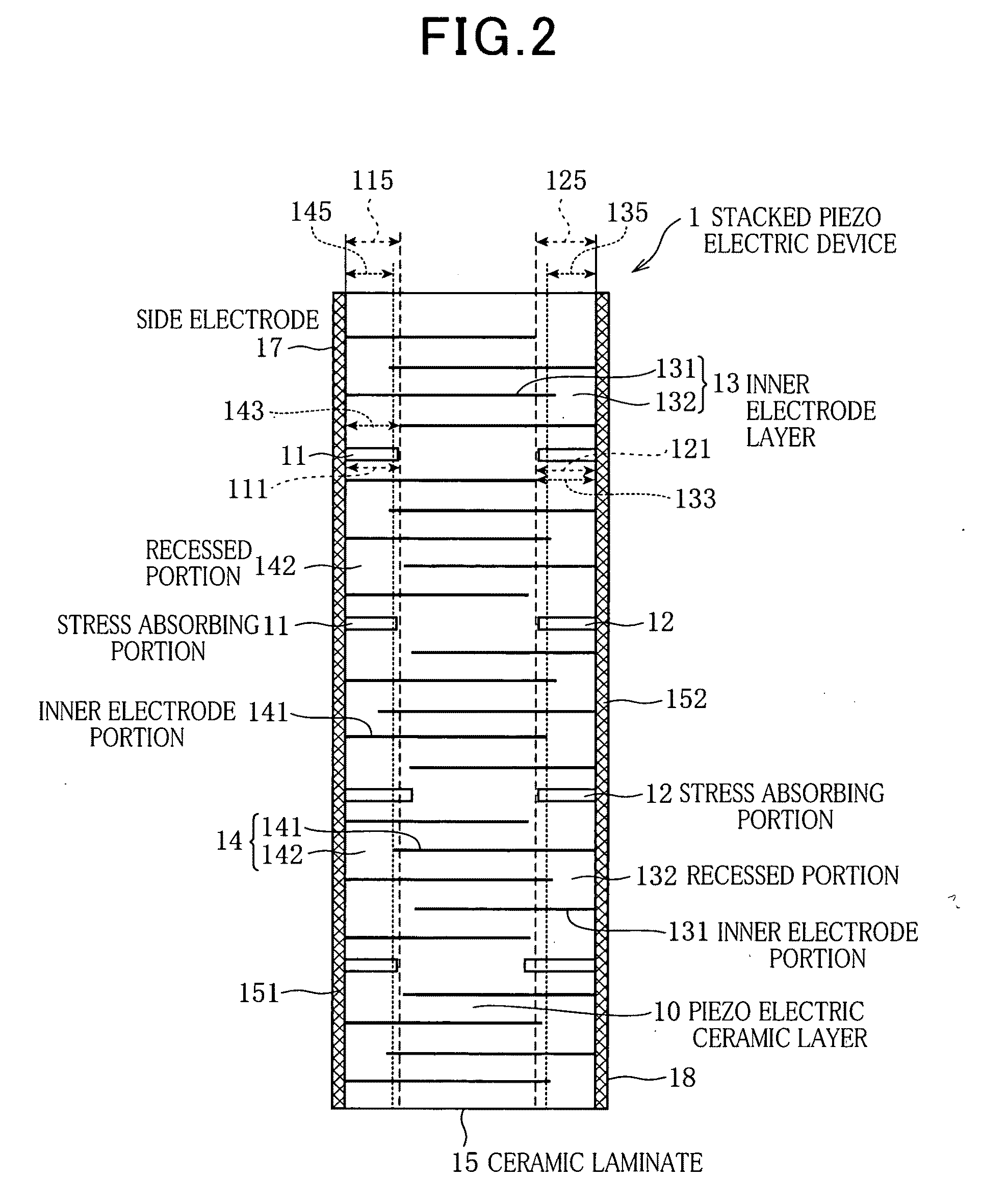
[0184]As illustrated in FIGS. 1 to 3, the stacked piezoelectric device 1 of this embodiment has a ceramic laminate 15 made by stacking the plurality of piezoelectric layers 10 and the plurality of inner electrode layers 13 and 14 alternately and the pair of side electrodes 17 and 18 fanned on side surfaces of the ceramic laminate 15. The inner electrode layers 13 and 14 include the conductive inner electrode portions 131 and 141 and the recessed portions 132 and 142 defined by retreating outer peripheral ends of the inner electrode portions 131 and 141 inwardly from the outer peripheral surface of the ceramic laminate 15. The inner electrode layers 13 and 14 are connected electrically to side electrodes 17 and 18, respectively, which are different from each other. Specifically, the inner electrode layers 13 and 14 are equipped with the inner ...

embodiment 2

[0237]Next, another variant of the stacked piezoelectric device of the invention will be described using FIGS. 18 to 27. The stacked piezoelectric device of this embodiment is a device in which the pattern in which the inner electrode portion and the recessed portion of the inner electrode layer is somewhat different from the embodiment 1.

[0238]As illustrated in FIGS. 18 to 20, the stacked piezoelectric device 1 of this embodiment, like in the embodiment 1, has the ceramic laminate 15 made by stacking the plurality of piezoelectric layers 10 and the plurality of inner electrode layers 13 and 14 alternately and the pair of side electrodes 17 and 18 formed on side surfaces of the ceramic laminate 15. The inner electrode layers 13 and 14 include the conductive inner electrode portions 131 and 141 and the recessed portions 132 and 142 defined by retreating outer peripheral ends of the inner electrode portions 131 and 141 inwardly from the outer peripheral surface of the ceramic laminate...

embodiment 3

[0292]Next, the stacked piezoelectric device according to the embodiment of the invention will be described using FIGS. 32 to 35.

[0293]As illustrated in FIGS. 32 to 34, the stacked piezoelectric device 1 of this embodiment, like in the embodiment 1, has the ceramic laminate 15 made by stacking the plurality of piezoelectric layers 10 and the plurality of inner electrode layers 23 and 24 alternately and the pair of side electrodes 17 and 18 formed on side surfaces of the ceramic laminate 15. The inner electrode layers 23 and 24 include the conductive inner electrode portions 231 and 241 and the recessed portions 232 and 242 defined by retreating outer peripheral ends of the inner electrode portions 231 and 241 inwardly from the outer peripheral surface of the ceramic laminate 15. The inner electrode layers 23 and 24 are connected electrically to side electrodes 17 and 18 alternately which are different from each other.

[0294]The ceramic laminate 15 has the stress absorbing portions 11...


PUM

PropertyMeasurementUnit
depthaaaaaaaaaa
depthaaaaaaaaaa
depthsaaaaaaaaaa

Abstract

A stacked piezoelectric device 1 including a ceramic laminate formed by laminating piezoelectric ceramic layers and inner electrode layers alternately and a pair of side electrodes. The inner electrode layers 13 and 14 have inner electrode portions 131 and 141 and the recessed portions 132 and 142. The ceramic laminate 15 has the stress absorbing portions 11 and 12. A recessed distance of one of two of the recessed portions 132 and 142 which interleave the stress absorbing portions 11 and 12 therebetween which is located on the same side surface as the stress absorbing portion 11 or 12 is greater than the depth of the stress absorbing portion 11 and 12.

Description

TECHNICAL FIELD[0001]The present invention relates to a stacked piezoelectric device equipped with a ceramic laminate made up of a plurality of piezoelectric ceramic layers and a plurality of inner electrode layers which are laminated alternately, a pair of side electrodes formed on side surfaces of the ceramic layer laminate, and stress absorbing portions formed in slit-like areas depressed inwardly into the sides of the ceramic laminate.BACKGROUND ART[0002]Conventionally, stacked piezoelectric devices are used as drive source of fuel injectors. The stacked piezoelectric device is made up of, for example, a ceramic laminate formed by stacking inner electrodes and piezoelectric ceramics alternately and a pair of outer electrodes connected to the inner electrode alternately.[0003]The stacked piezoelectric device is used in severe environmental conditions over a long duration, especially when employed in fuel injectors. Therefore, in order to improve the electric insulation of the sid...

Claims


Application Information

Patent Timeline
Patent Type & Authority Applications(United States)
IPC IPC(8): F02M51/06H01L41/083H01L41/187H01L41/22H01L41/27H01L41/293H01L41/297H01L41/39
CPCF02M63/0026H01L41/273H01L41/0838H10N30/508H10N30/053
Inventor SUZUKI, SATOSHIMURAI, ATSUSHIASANO, HIROAKINODA, KOUJINAGAYA, TOSHIATUIWASE, AKIOFUJII, AKIRAKADOTANI, SHIGE
Owner DENSO CORP
Why Eureka
Try Eureka