Resistance change memory

a technology of resistance change and memory, applied in the field of resistance change memory, can solve the problems of increasing the chip area, increasing the manufacturing cost, and the inability to partially activate one word line in the memory cell array

Inactive Publication Date: 2010-06-24
KK TOSHIBA
View PDF5 Cites 79 Cited by
  • Summary
  • Abstract
  • Description
  • Claims
  • Application Information

AI Technical Summary

Benefits of technology

[0026]FIG. 12 is a diagram showing the structure of a resistance change memory element; and
[0027]FIG. 13 is a diagram showing the structure of the resistance change memory element.

Problems solved by technology

Therefore, in the DRAM, it is impossible to partially activate one word line in the memory cell array owing to the specifications of the operation of the word line.
That is, the defective cells increase with the capacity enlargement and the size miniaturization of the memory, but in such a case, the improvement of the remedy efficiency of the defective cells may cause the increase of a chip area and the increase of a manufacturing cost.

Method used


Image

  • Resistance change memory
  • Resistance change memory
  • Resistance change memory

Examples


first embodiment

[0029]Hereinafter, a first embodiment of the present invention will be described with reference to FIGS. 1 to 8.

[0030](1) Basic Constitution

[0031]The basic constitution of a resistance variable semiconductor memory according to a first embodiment of the present invention will be described with reference to FIGS. 1 and 2.

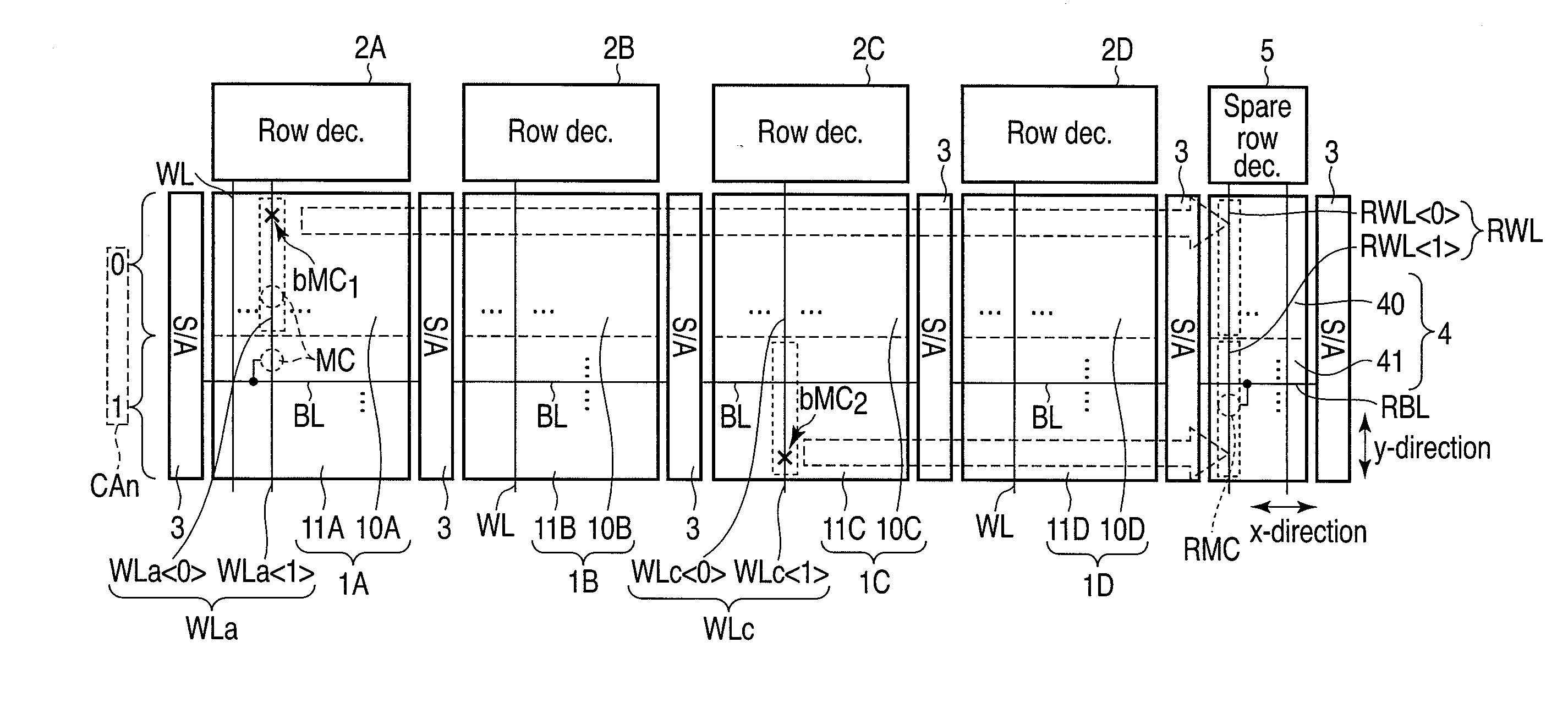
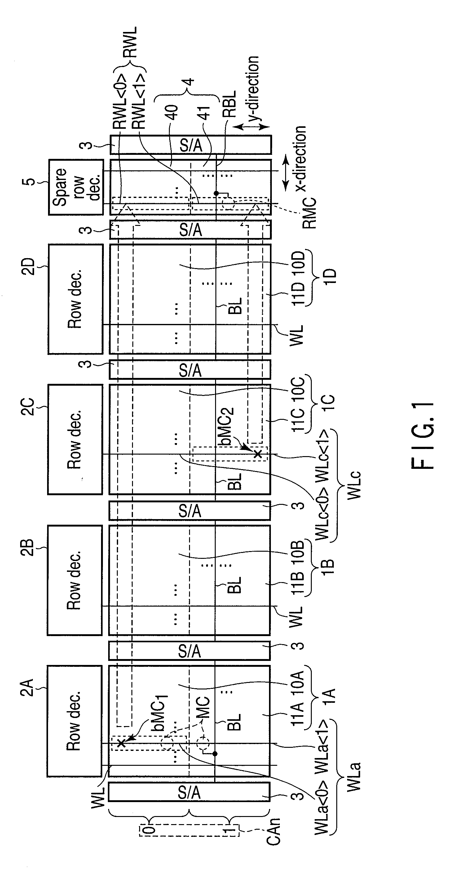
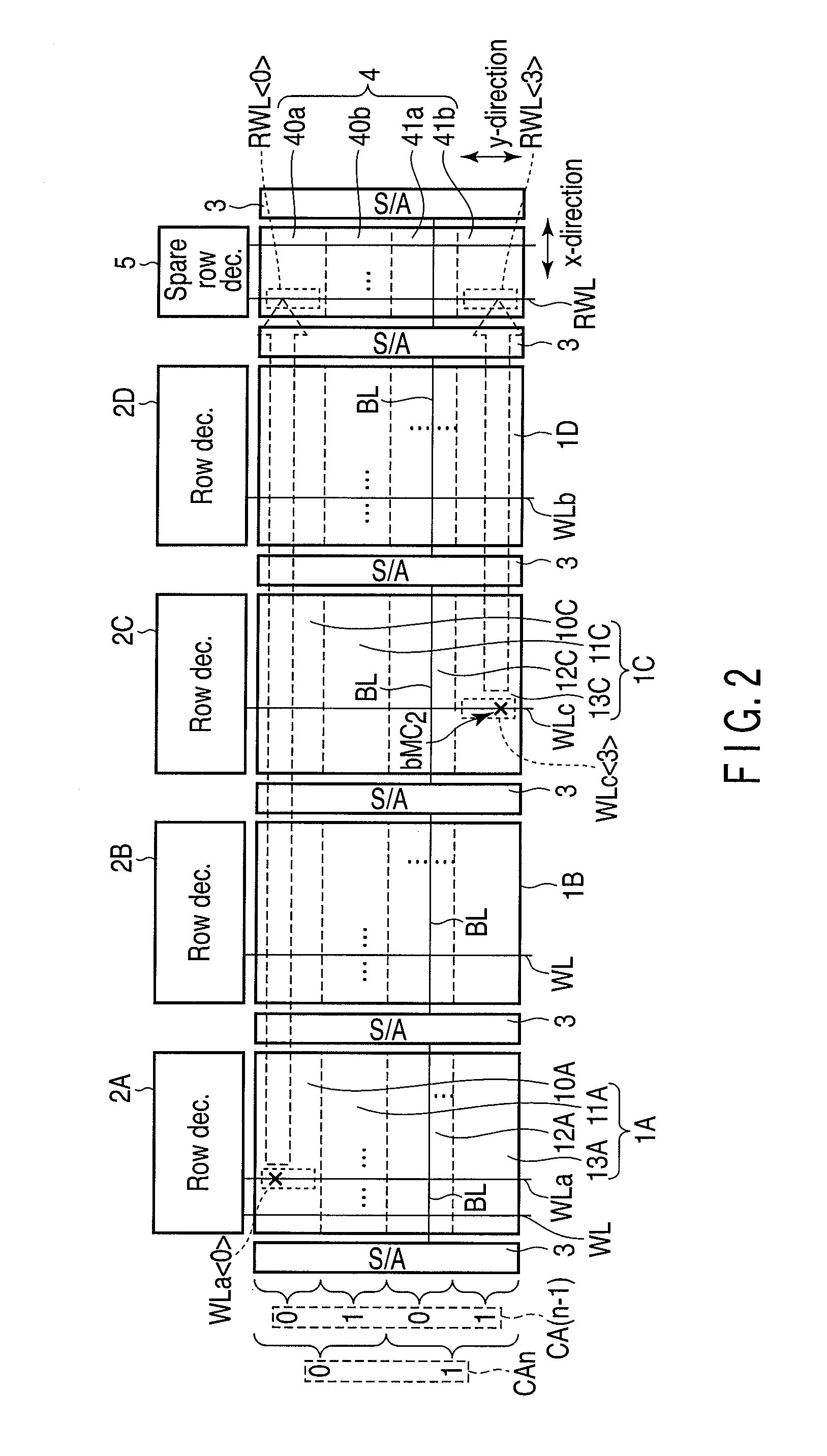
[0032]FIG. 1 shows the constitution of memory cell arrays and circuits arranged near the arrays in the resistance variable semiconductor memory according to the present embodiment.

[0033]In an example shown in FIG. 1, four memory cell arrays 1A to 1D are provided in a chip. However, one memory cell array may be provided in one chip.

[0034]The memory cell arrays 1A to 1D include a plurality of memory cells MC using resistance change memory elements. The plurality of memory cells MC are arrayed in the memory cell arrays 1A to 1D.

[0035]In the memory cell arrays 1A to 1D, a plurality of word lines WL and a plurality of bit lines BL are provided. In FIG. 1, the word lines W...

second embodiment

[0245]A second embodiment of the present invention will be described with reference to FIGS. 10 and 11. Note that in FIGS. 10 and 11, substantially the same constituent elements as those of the first embodiment are denoted with the same reference numerals, and the detailed description thereof is performed if necessary.

[0246]FIG. 10 shows a circuit constitution near memory cell arrays of a semiconductor memory having a word line constitution referred to as a hierarchical word line system.

[0247]In memory cell arrays 9A to 9D of the hierarchical word line system shown in FIG. 10, the word line constitution has two classes. Therefore, each word line of the present embodiment includes a main word line MWL and a sub-word line SWL connected to the main word line MWL.

[0248]The memory cell arrays 9A to 9D include a plurality of physically divided regions 90A to 90D, 91A to 91D. In the present embodiment, the physically divided regions 90A to 90D, 91A to 91D will be referred to as the blocks ...


PUM


Abstract

A resistance change memory of an aspect of the present invention including memory cells including resistance change memory element, word lines connected to the memory cells, a row decoder which activates the word lines, redundant cells used instead of defective cells, a redundant word line connected to redundant cells, a redundant row decoder which activates the redundant word line, a control circuit in which defect address information indicating the word line connected to the defective cell is stored and which remedies the defective cell, and regions provided in a memory cell array and a redundant cell array and identified based on column address information, wherein the control circuit replaces a part of the word line connected to the defective cell with a part of the redundant word line in accordance with each of the regions, and allows the redundant row decoder to activate the replaced redundant word line.

Description

CROSS-REFERENCE TO RELATED APPLICATIONS[0001]This application is based upon and claims the benefit of priority from prior Japanese Patent Application No. 2008-324322, filed Dec. 19, 2008, the entire contents of which are incorporated herein by reference.BACKGROUND OF THE INVENTION[0002]1. Field of the Invention[0003]The present invention relates to a resistance change memory. In particular, it relates to a defect remedy technology of a resistance change memory.[0004]2. Description of the Related Art[0005]In recent years, with the popularization of cellular phones and portable audio players, semiconductor memories have been mounted in such electronic devices.[0006]In the semiconductor memory, a redundant cell array of an arbitrary scale is provided in the same chip as that of a memory cell array to remedy a defective cell in the memory cell array. For the semiconductor memory, there is employed a technique for remedying the defect of memory cells by using redundant cells in this redu...

Claims


Application Information

Patent Timeline
Patent Type & Authority Applications(United States)
IPC IPC(8): G11C11/00G11C29/00G11C5/02G11C8/00
CPCG11C8/08G11C11/16G11C13/0004G11C13/0007G11C13/0028G11C2213/32G11C29/789G11C29/81G11C2029/1208G11C2213/31G11C29/4401G11C11/1653G11C11/1659G11C11/1673G11C11/1675G11C11/1693
Inventor TSUCHIDA, KENJI
Owner KK TOSHIBA
Why Eureka
Try Eureka