Capacitive touch panel
a capacitance touch panel and capacitive technology, applied in the field of capacitive touch panel, can solve the problems of poor horizontal capacitance detection, and achieve the effect of reducing mutual interference and high sensitivity
- Summary
- Abstract
- Description
- Claims
- Application Information
AI Technical Summary
Benefits of technology
Problems solved by technology
Method used
Image
Examples
Embodiment Construction
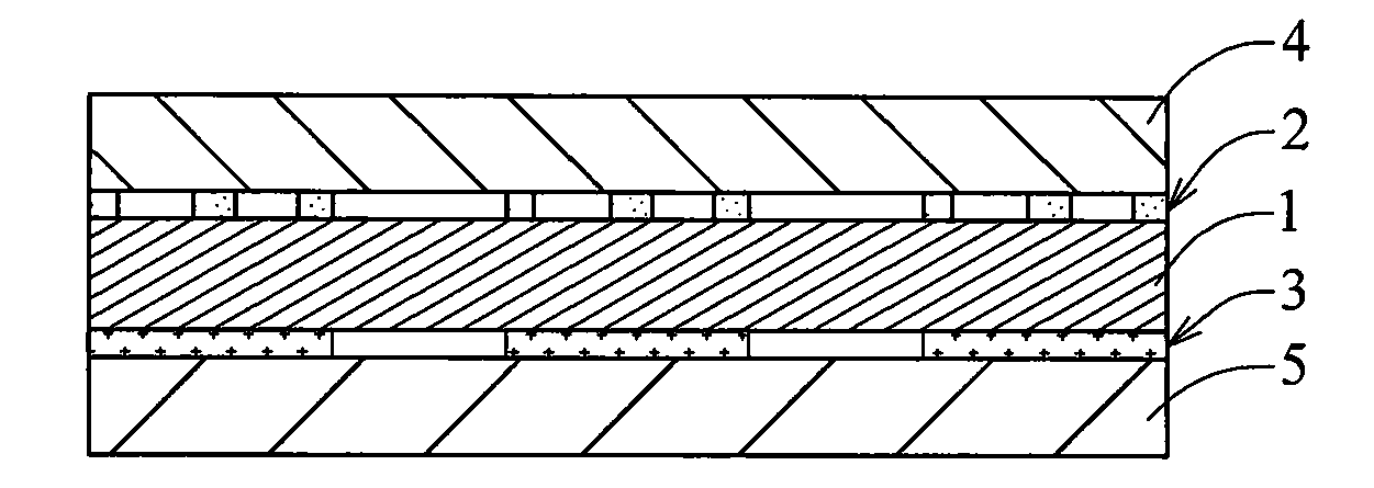
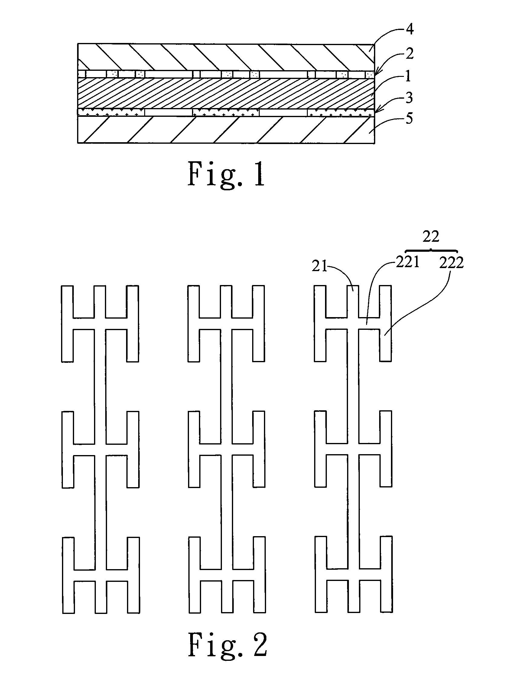
[0022]FIG. 1 is a sectional view diagram illustrating a capacitive touch panel according to one embodiment of the present invention. The capacitive touch panel includes an insulating layer 1, a plurality of first dimensional conductive patterns, e.g. column conductive patterns 2, and a plurality of second dimensional conductive patterns, e.g. row conductive patterns 3. The column conductive patterns 2 are configured over an upper surface of the insulating layer 1, and the row conductive patterns 3 are configured over a lower surface of the insulating layer 1. The capacitive touch panel also includes an upper insulating layer 4 configured over the column conductive patterns 2 and a lower insulating layer 5 configured over the row conductive patterns 3. The upper insulating layer 4 and the lower insulating layer 5 are used for reducing the possibility of wearing caused by, for example, human touch. The column conductive patterns 2 over the upper surface and the row conductive patterns...
PUM
 Abstract
Description
Claims
Application Information


