Supercharge Your Innovation With Domain-Expert AI Agents!

Binning Circuit and Method for an Image Sensor

a technology of image sensor and circuit, applied in the field of image sensor, can solve the problems of signal collision, inability to effectively binn signals across different sharing groups in a conventional vertical sharing image sensor, and disadvantageous limitation of signals of conventional multiple-vertical-pixel-sharing image sensor. achieve the effect of effectively binning signals across different sharing groups

Active Publication Date: 2010-08-05
HIMAX IMAGING LIMITED
View PDF2 Cites 6 Cited by
  • Summary
  • Abstract
  • Description
  • Claims
  • Application Information

AI Technical Summary

Benefits of technology

[0009]In view of the foregoing, it is an object of the present invention to provide a binning circuit and method for an image sensor, particularly a multiple-vertical-pixels-sharing image sensor, for effectively binning signals across different sharing groups.

Problems solved by technology

Nevertheless, binning signals across different sharing groups in a conventional vertical sharing image sensor become difficult without using additional circuitry.
However, turning on the transfer gates (tx_A_n, tx_B_n, n=1, 2, etc.) from both the group A and the group B in the same (vertical) column at the same time will catastrophically result in signal collision between / among the outputs of the groups A and B at the column node (col).
As a result, the conventional multiple-vertical-pixels-sharing image sensor disadvantageously has a limited number of signals to be binned.

Method used


Image

  • Binning Circuit and Method for an Image Sensor
  • Binning Circuit and Method for an Image Sensor
  • Binning Circuit and Method for an Image Sensor

Examples


Embodiment Construction

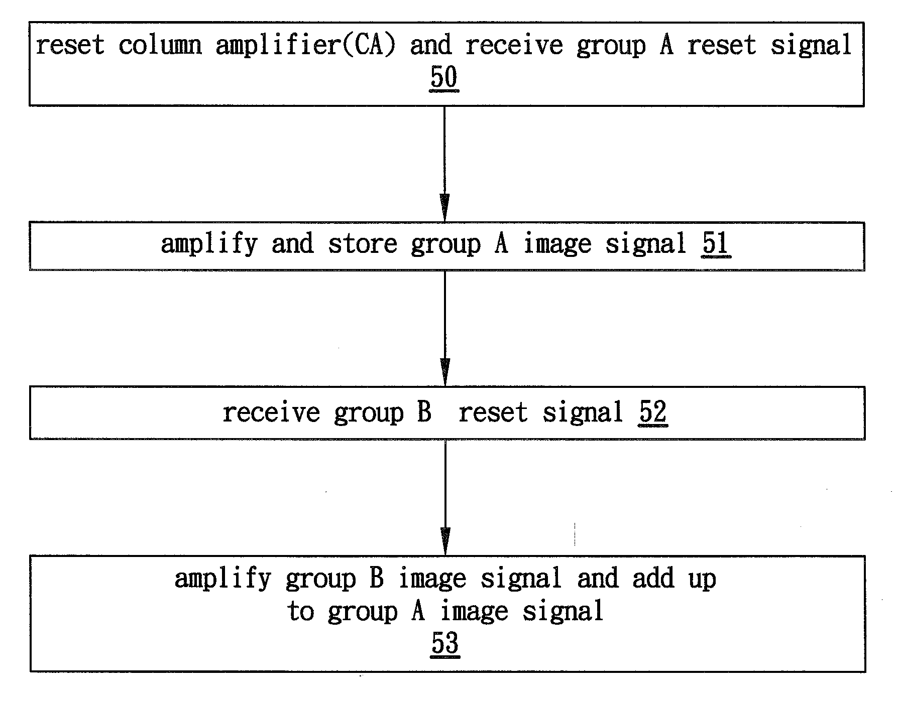
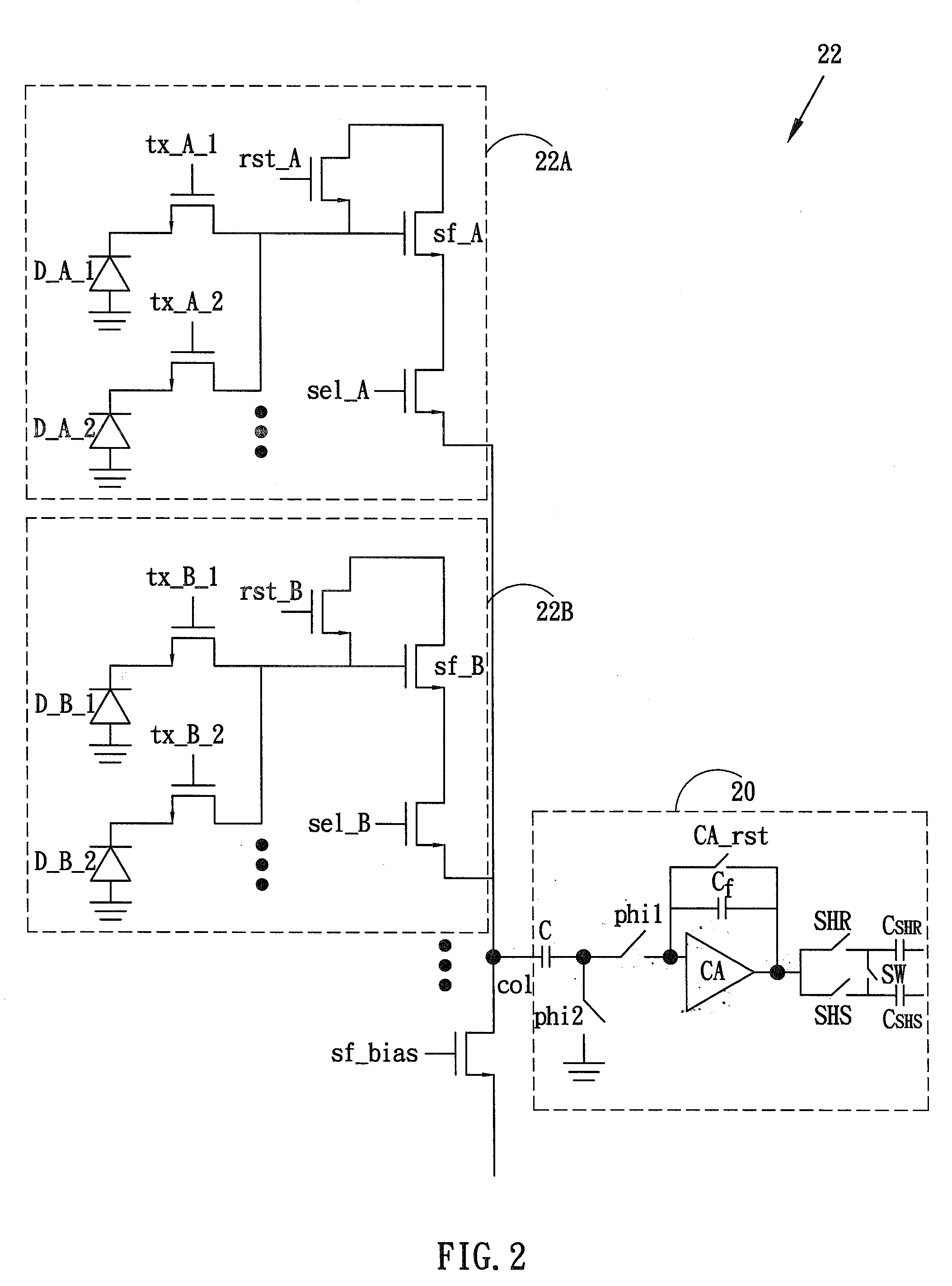
[0017]FIG. 2 shows a binning circuit 20 for a multiple-vertical-pixels-sharing image sensor 22 according to one embodiment of the present invention. The multiple-vertical-pixels-sharing image sensor 22 includes multiple groups, such as group A (22A) and group B (22B), and each group shares associated common circuitry arranged in a vertical sharing manner. The image sensor 22 may be, but is not limited to, a charge-coupled device (CCD) or complementary metal-oxide-semiconductor (CMOS) sensor for converting images of visible light into electronic signals. The output of the binning circuit 20 may be fed to an amplifier (not shown), such as a programmable gain amplifier (PGA). The disclosed image sensor 22 with the binning circuit 20 may be generally applied in a digital image processing device, such as, but not limited to, cameras or camcorders.

[0018]Specifically, taking the group A (22A) for example, each group of the image sensor 22 includes a reset transistor rst_A, a source followe...


PUM


Abstract

A binning circuit and method for an image sensor is disclosed. A column amplifier (CA) is first reset, and thus generates a CA reset signal. A capacitor and a switch network are coupled between an output of the image sensor and an input of the column amplifier. A correlated double sampling (CDS) circuit controllably receives the output of the column amplifier. The switch network is controlled in a way such that an image signal of a first group of the image sensor is transmitted and stored in the CDS circuit, and an image signal of a second group is then added to the stored image signal of the first group.

Description

BACKGROUND OF THE INVENTION[0001]1. Field of the Invention[0002]The present invention generally relates to an image sensor, and more particularly to a binning circuit and method for a multiple-vertical-pixels-sharing image sensor.[0003]2. Description of the Prior Art[0004]Semiconductor based image sensors, such as charge-coupled devices (CCDs) or complementary metal-oxide-semiconductor (CMOS) sensors, are widely used, for example, in cameras or camcorders, to convert images of visible light into electronic signals that can then be stored, transmitted or displayed.[0005]Some of the pixels (or photodiodes) in the image sensor can commonly share a circuit to reduce the overall size. The sharing structure may either be arranged in a vertical manner in which the pixels in the same column are sharing common circuitry, or in a horizontal manner in which the pixels in the same row are sharing common circuitry. FIG. 1 shows a conventional multiple-vertical-pixels-sharing image sensor 10, in ...

Claims


Application Information

Patent Timeline
Patent Type & Authority Applications(United States)
IPC IPC(8): H04N5/335
CPCH04N5/347H04N5/37457H04N5/3575H04N25/46H04N25/616H04N25/778
Inventor CHIU, BOH-SHUNYIN, PING-HUNG
Owner HIMAX IMAGING LIMITED
Features
  • R&D
  • Intellectual Property
  • Life Sciences
  • Materials
  • Tech Scout
  • Unparalleled Data Quality
  • Higher Quality Content
  • 60% Fewer Hallucinations
Learn More