
Eureka
For R&D, Eureka makes reading and utilizing patents & technical documents easy.
Eureka AIR
Designed for self-driven R&D workflows. Generate viable solutions, solve complex R&D challenges, empower your innovation with AI.

Eureka Materials
Designed for material experts only. Revolutionize your material R&D, from search, analyze, to developing new materials.

TechResearch
Generate reliable direction feasibility study reports for your R&D in just a few steps.

TechSeek
Discover and master advanced knowledge NOW. Basics, ideas, possibilities, all at once.

TechMind
As an expert in R&D Theories, TechMind can generates customized viable solutions instantly.

TechRisk
Analyze your overall solution with one click, know your potential R&D risks in advance.

TechMonitor
Get weekly tech updates, stay abreast of the latest tech innovations and key insights.
Photoconductor system for electrophotographic device
- Summary
- Abstract
- Description
- Claims
- Application Information
AI Technical Summary
Problems solved by technology
Method used
Image

Examples
example
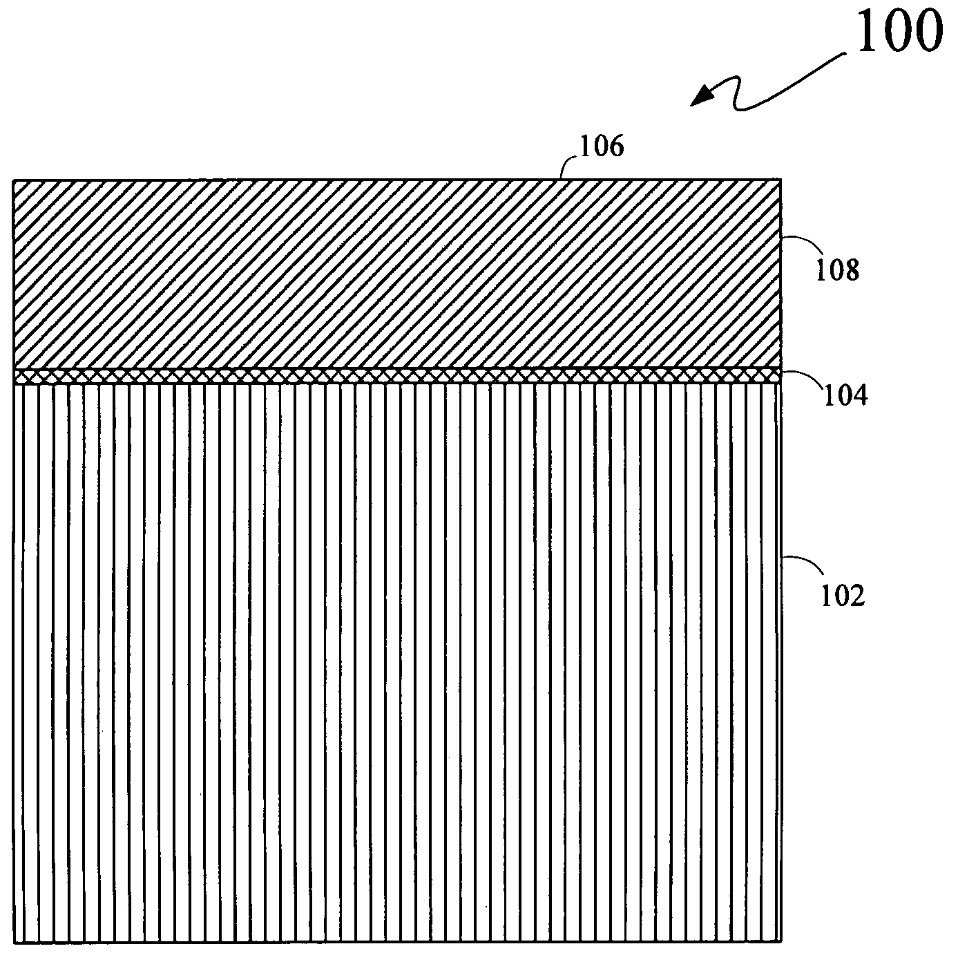
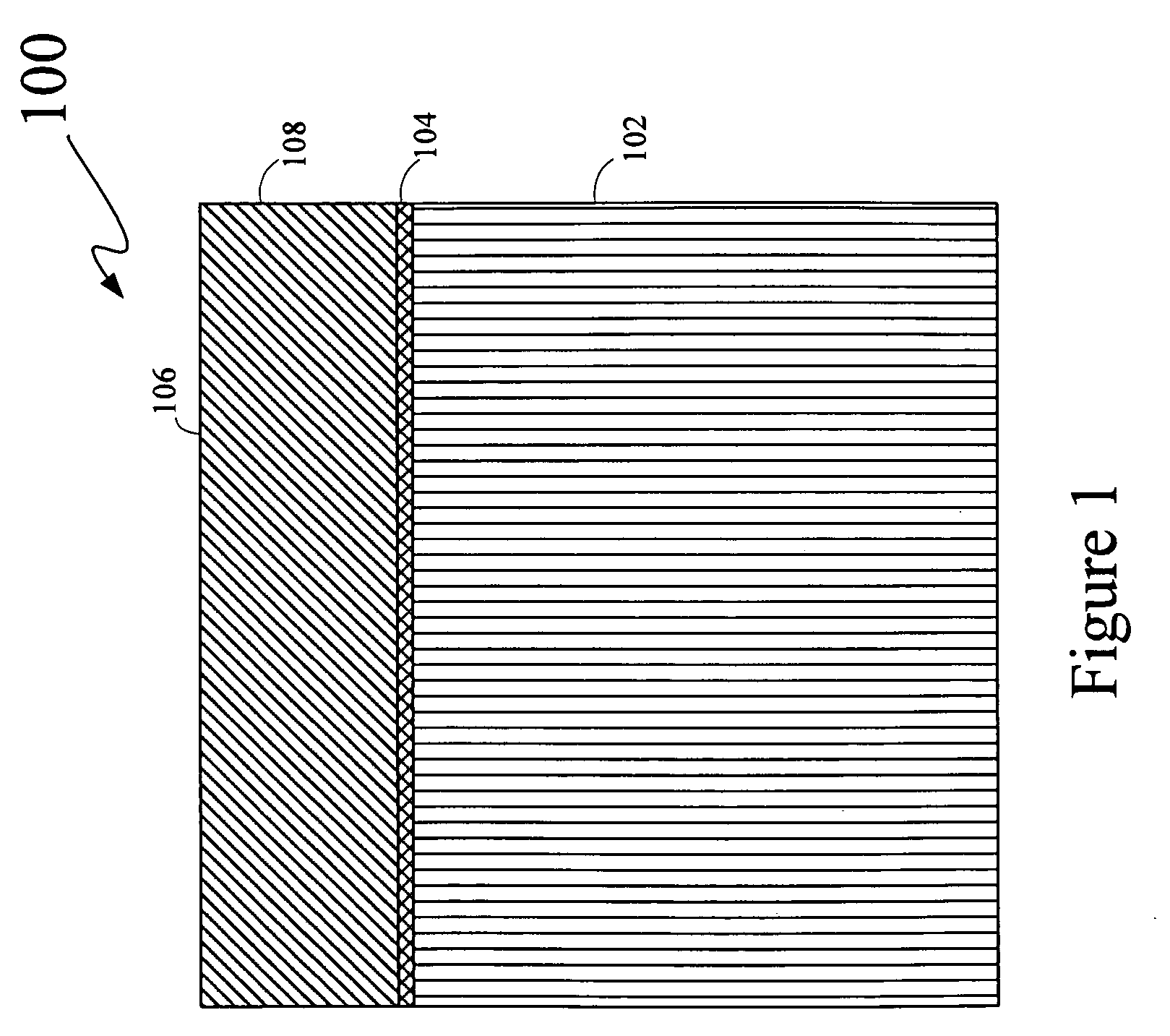
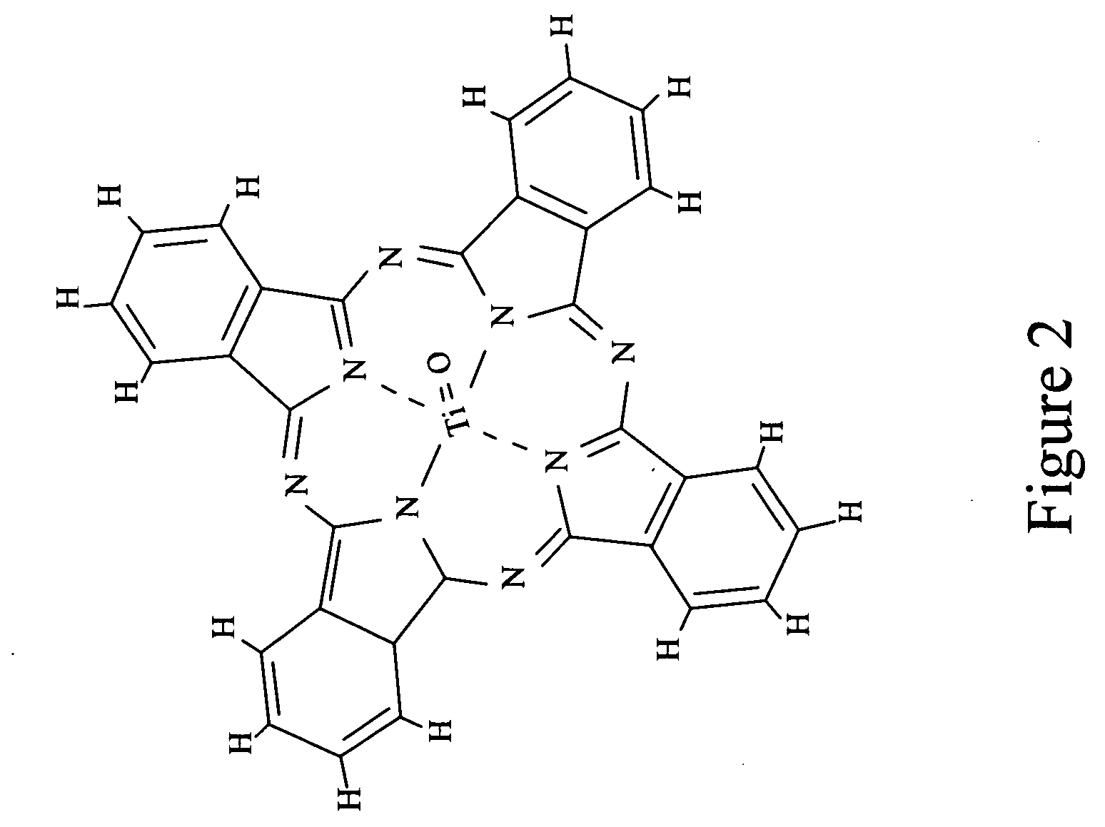
[0050]In the following example, different electrophotographic photoconductor systems were investigated for use in an electrophotographic device. Each of the different electrophotographic photoconductor systems was prepared by coating a charge generation layer and a charge transport layer onto an electroconductive support (such as an anodized aluminum drum). More specifically, the charge generation layer (in the form of a liquid dispersion) was coated onto the electroconductive support using a dip-coating technique, and then air-dried. The charge generation layer included one or more crystalline forms of TiOPC, such as type IV TiOPC; polyvinylbutyral, poly(methylphenylsiloxane) (PMPS); poly(4-hydroxystyrene) (PHS); and terphenyl additive, in a 92:8 methyl ethyl ketone (MEK) / cylcohexane mixture prepared in an Eiger mill with a final particle size of about 0.17 microns (as explained in Table 1).
[0051]Further, the charge transport layer (in the form of a liquid solution) was coated onto...
PUM
| Property | Measurement | Unit |
|---|---|---|
| Nanoscale particle size | aaaaa | aaaaa |
| Nanoscale particle size | aaaaa | aaaaa |
| Wavelength | aaaaa | aaaaa |
Abstract
Description
Claims
Application Information
 - R&D Engineer
- R&D Manager
- IP Professional
- Industry Leading Data Capabilities
- Powerful AI technology
- Patent DNA Extraction
Browse by: Latest US Patents, China's latest patents, Technical Efficacy Thesaurus, Application Domain, Technology Topic, Popular Technical Reports.
© 2024 PatSnap. All rights reserved.Legal|Privacy policy|Modern Slavery Act Transparency Statement|Sitemap|About US| Contact US: help@patsnap.com