Impedance control circuit and semiconductor device including the same

a technology of impedance control circuit and semiconductor device, applied in the direction of oscillator, pulse technique, instruments, etc., to achieve the effect of accurate impedance control operation and reduction of impedance adjustment error

Active Publication Date: 2010-08-19
LONGITUDE LICENSING LTD
View PDF14 Cites 14 Cited by
  • Summary
  • Abstract
  • Description
  • Claims
  • Application Information

AI Technical Summary

Benefits of technology

[0019]According to the present invention, the adjust error generated by the first replica circuit and the adjust error generated by the second replica circuit cancel each other. This can reduce the impedance adjust error of the second replica circuit impedance controlled based on the impedance of the first replica circuit. Accordingly, the present invention can ensure a more accurate impedance control operation.

Problems solved by technology

Therefore, the impedances of the replica circuits after the impedance control often include adjust errors with respect to the target impedances, respectively.
In this way, the conventional impedance control circuit has the problem that the pull-down replica circuit is greater in the adjust error than the pull-up replica circuit and the adjust error of the pull-down replica circuit reaches up to two bit of the count value.
This problem occurs not only to a case that the impedances of both the pull-up and pull-down replica circuits at the start of impedance control are lower than the target impedances, respectively but also to an opposite case, that is, a case that the impedances of both the pull-up and pull-down replica circuits at the start of the impedance control are higher than the target impedances, respectively.

Method used


Image

  • Impedance control circuit and semiconductor device including the same
  • Impedance control circuit and semiconductor device including the same
  • Impedance control circuit and semiconductor device including the same

Examples


first embodiment

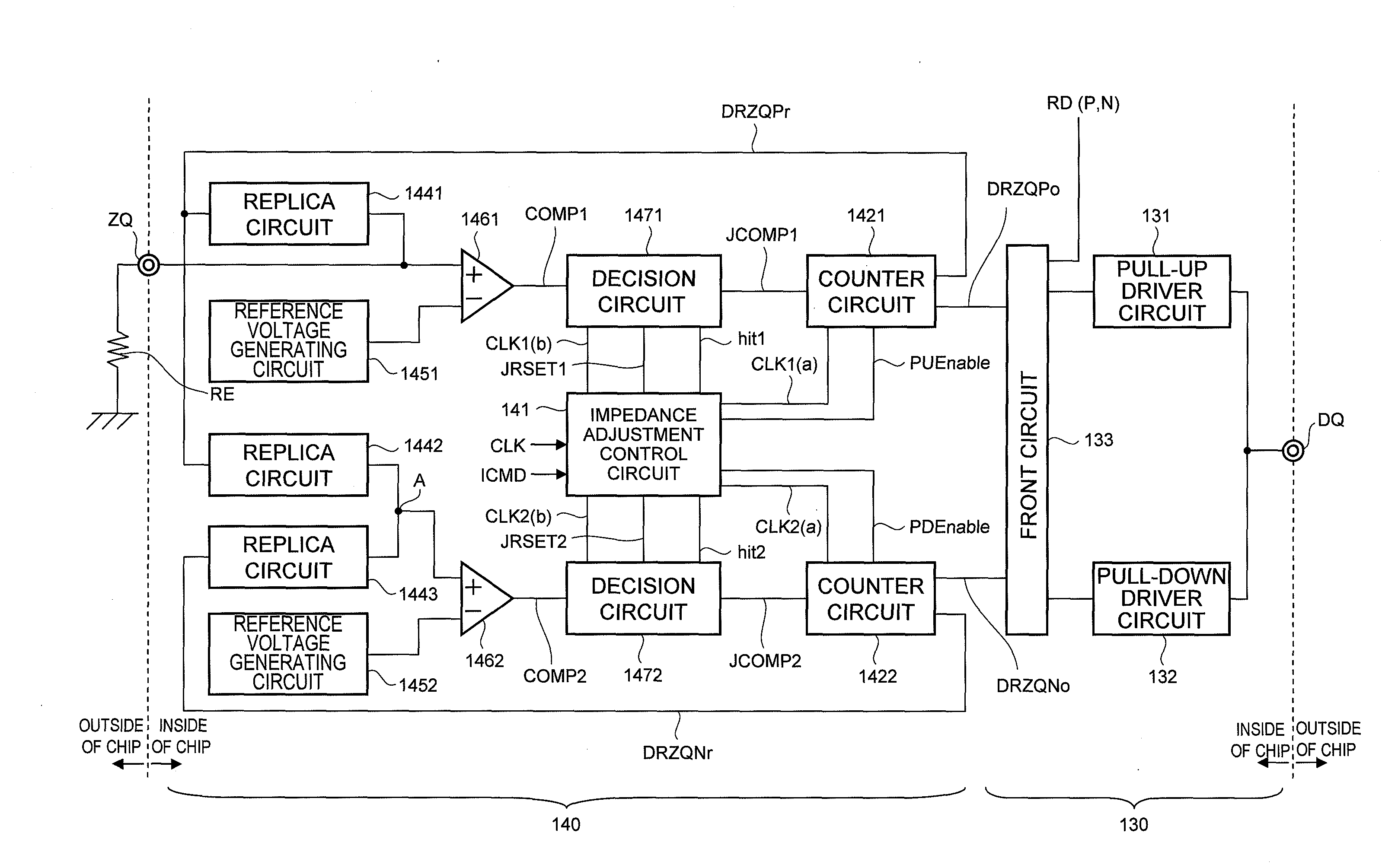
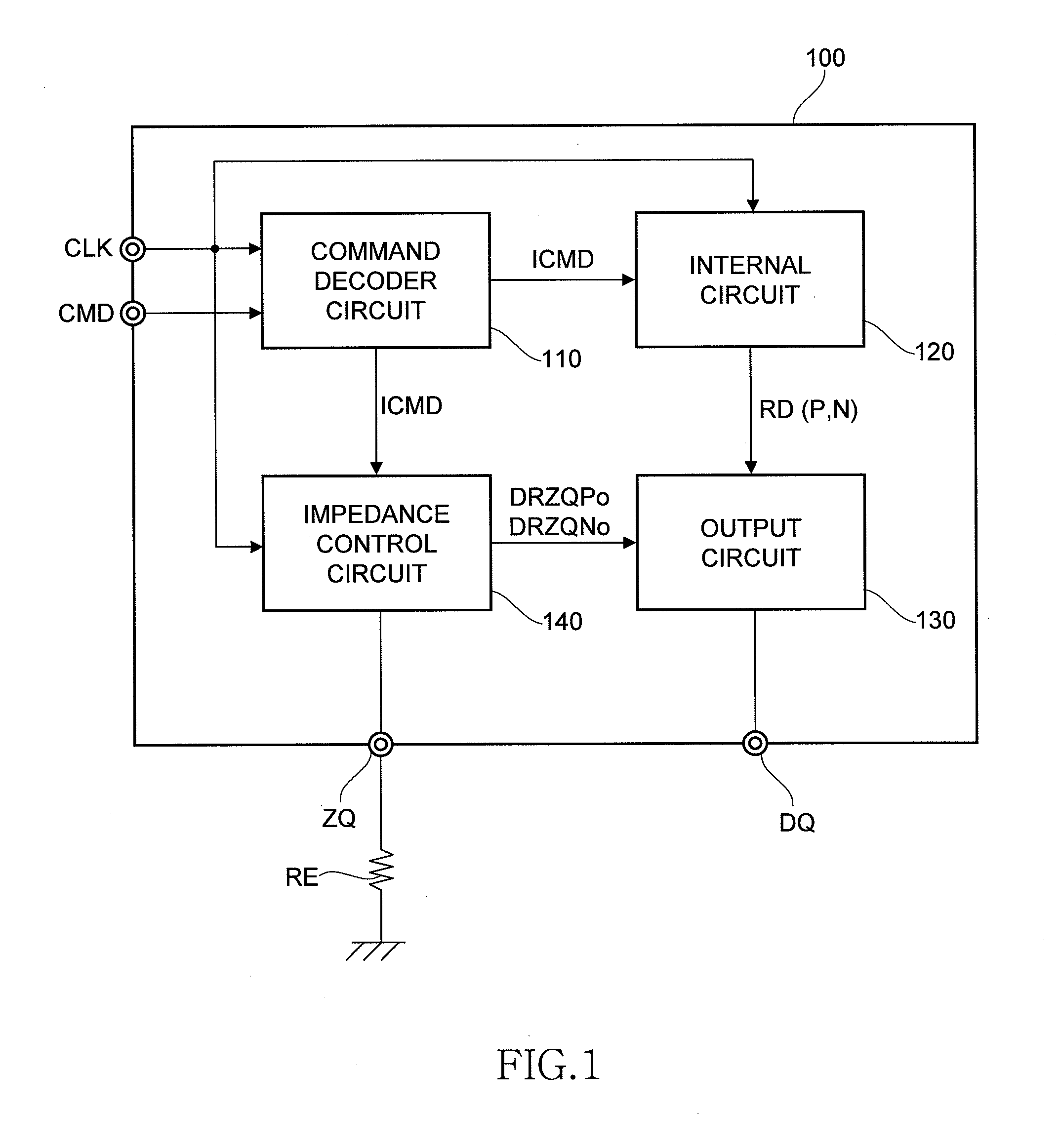
[0047]FIG. 1 is a block diagram showing a configuration of principal parts of a semiconductor device 100 according to the present invention.

[0048]As shown in FIG. 1, the semiconductor device 100 according to the first embodiment includes a clock terminal CLK, a command terminal CMD, a command decoder circuit 110, an internal circuit 120, an output circuit 130, an impedance control circuit 140, an output terminal DQ, and a calibration terminal ZQ. An external resistor RE is connected to the calibration terminal ZQ.

[0049]The clock terminal CLK is input a clock signal from an outside. The command terminal CMD is input a command signal for controlling the internal circuit 120 and the impedance control circuit 140.

[0050]The command decoder circuit 110 fetches in the command signal synchronously with the clock signal, decodes the command signal, and generates an internal command signal ICMD indicating an operation corresponding to the input command signal. The internal command ICMD is sup...

second embodiment

[0112]A second embodiment according to the present invention described next is an example in which an impedance control circuit is configured to make it difficult to influence noise on an impedance control circuit.

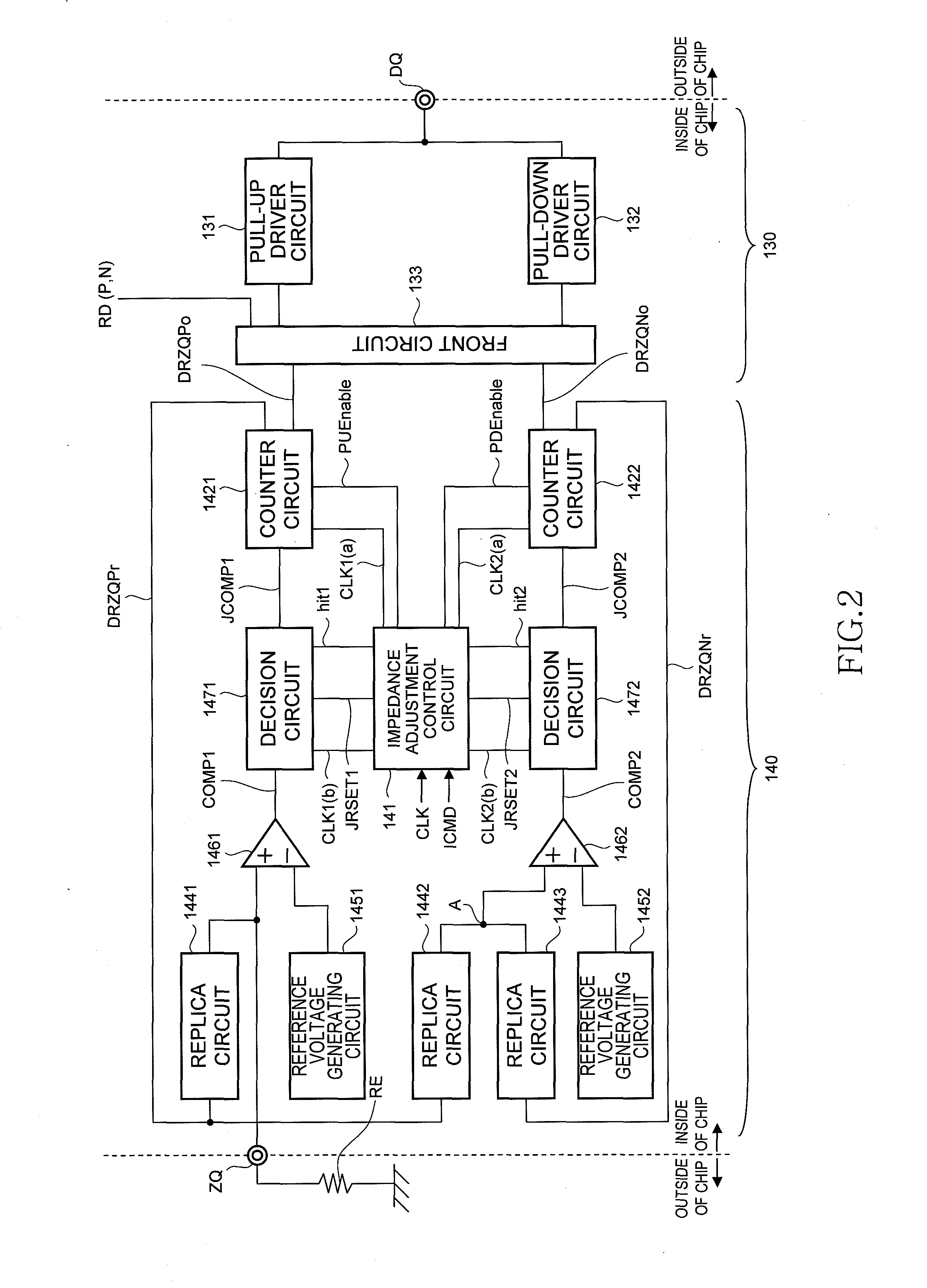
[0113]The overall configuration of the impedance control circuit according to the second embodiment is not shown herein. However, the impedance control circuit according to the second embodiment is different from the impedance control circuit 140 according to the first embodiment such that decision circuits 2471 and 2472 are used instead of the decision circuits 1471 and 1472 shown in FIG. 2, respectively.

[0114]FIG. 13 is a circuit diagram of the decision circuits 2471 and 2472.

[0115]As shown in FIG. 13, the decision circuits 2471 and 2472 are the same in circuit configuration. Each of the decision circuits 2471 and 2472 includes three flip-flop circuits 71 to 73 cascaded to one another, an inverter circuit 74, and a NAND circuit 75. By so configuring as shown in FIG. 13, ...

third embodiment

[0130]A third embodiment according to the present invention is intended to solve the problems described above. That is, the third embodiment is an embodiment of an impedance control circuit that makes the time required for hit determination constant regardless of whether the impedance of the replica circuit 1441 at start of the impedance control is higher or lower than that of the external resistor RE.

[0131]The overall configuration of the impedance control circuit according to the third embodiment is not shown herein. However, the impedance control circuit according to the third embodiment is different from the impedance control circuit 140 according to the first embodiment such that a decision circuit 347 is used instead of the decision circuits 1471 and 1472 shown in FIG. 2.

[0132]FIG. 17 is a circuit diagram of the decision circuit 347.

[0133]As shown in FIG. 17, the decision circuit 347 includes decision circuits 2471a, 3471, 2472a, and 3472, a switch unit 3473, and an AND circui...


PUM


Abstract

To include two counter circuits that change impedances of two replica circuits, respectively, and an impedance adjustment control circuit that controls the counter circuits to update count values of the counter circuits. The impedance adjustment control circuit controls one of the counter circuits to finish updating the count value of the counter circuit in response to a change of the impedance of the corresponding replica circuit from a state of being lower than an impedance of an external resistor to a state of being higher than the impedance of the external resistor, and controls the other counter circuit to finish updating the count value of the other counter circuit in response to a change of the impedance of the other replica circuit from a state of being higher than the impedance of the former replica circuit to a state of being lower than the impedance of the former replica circuit. With this configuration, the adjust errors generated in the replica circuits are canceled.

Description

BACKGROUND OF THE INVENTION[0001]1. Field of the Invention[0002]The present invention relates to an impedance control circuit, and more particularly relates to an impedance control circuit that adjusts an impedance of an output buffer provided in a semiconductor device. The present invention also relates to a semiconductor device including such an impedance control circuit.[0003]2. Description of Related Art[0004]Recently, a very high data transfer rate is required to transfer data between semiconductor devices (for example, between a CPU and a memory). To realize this very high transfer rate, amplitudes of input and output signals are increasingly set lower. Lower amplitudes of input and output signals make required accuracy of an impedance of an output buffer quite higher.[0005]The impedance of the output buffer is influenced by not only manufacturing process conditions but also a surrounding temperature or a power supply voltage. Due to this, when the output buffer is required to...

Claims


Application Information

Patent Timeline
Patent Type & Authority Applications(United States)
IPC IPC(8): G05F3/00
CPCH03K19/017581H03K19/0005
Inventor KUWAHARA, SHUNJIFUJISAWA, HIROKI
Owner LONGITUDE LICENSING LTD
Why Eureka
Try Eureka