

Solid-state imaging device, method of manufacturing the same, and electronic apparatus
a technology of solid-state imaging and electronic equipment, which is applied in the direction of optical elements, instruments, television systems, etc., can solve the problems of difficult to dramatically suppress the occurrence of flares or ghosts, and achieve the effect of improving picture image quality
- Summary
- Abstract
- Description
- Claims
- Application Information
AI Technical Summary
Benefits of technology
Problems solved by technology
Method used
Image

Examples
first embodiment
1. Example of Solid-state Imaging Device
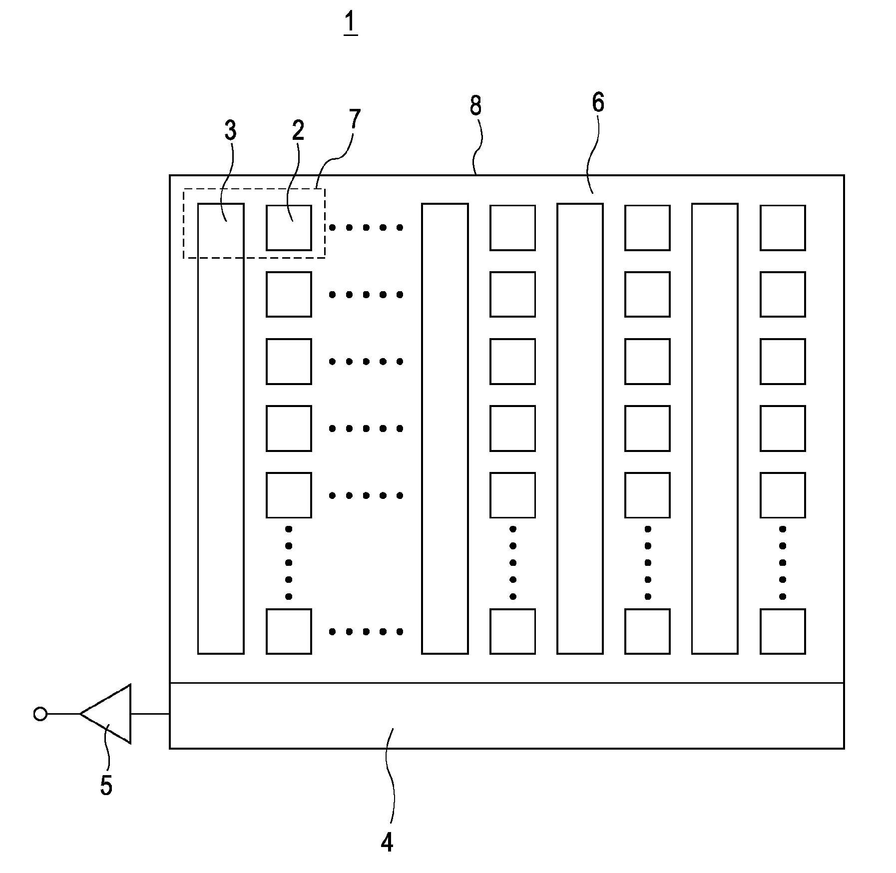
[0043]1.1 Schematic Configuration of the Whole Solid-state Imaging Device
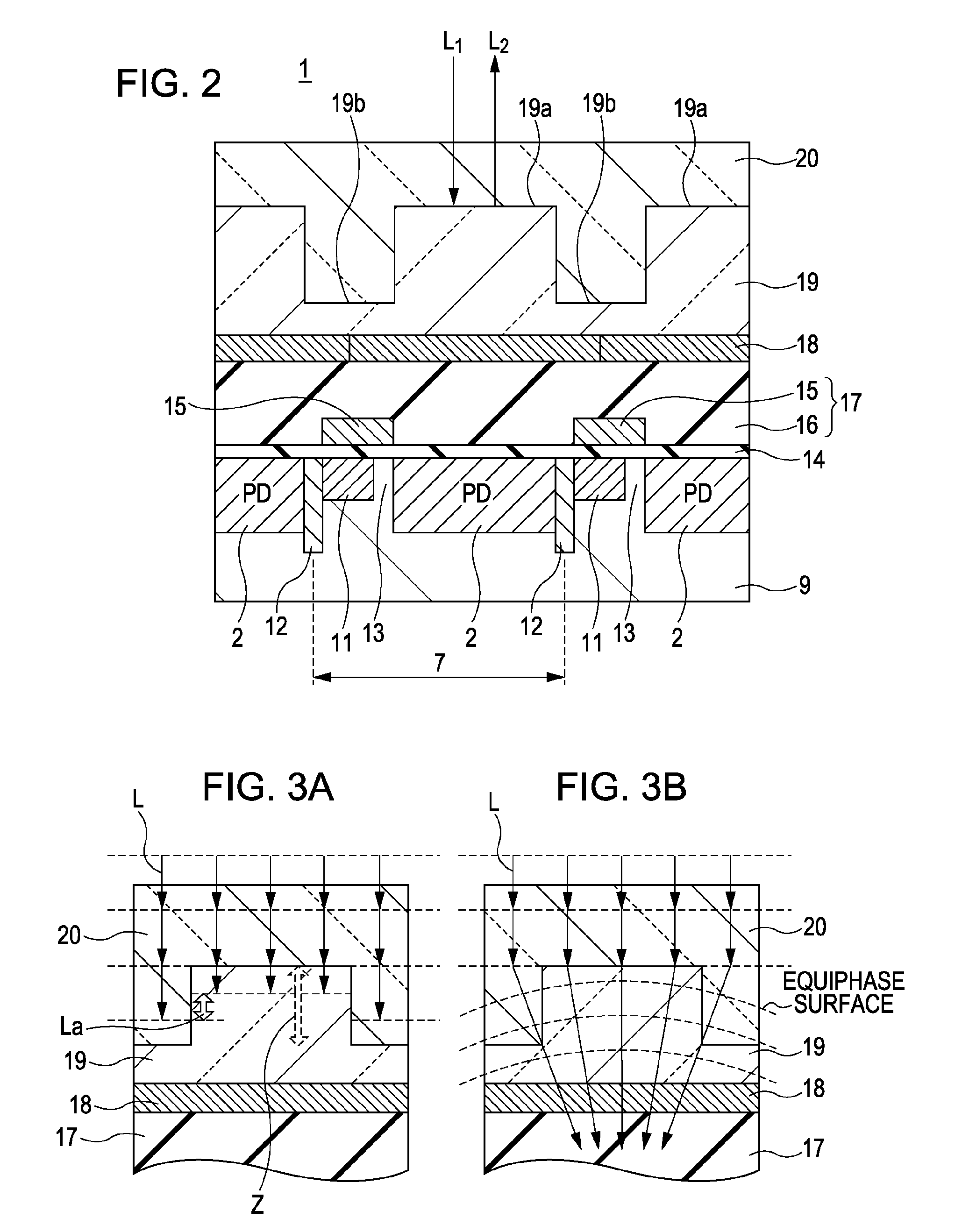
[0044]1.2 Sectional Configuration of the Solid-state Imaging Device
[0045]1.3 Method of manufacturing the Solid-state Imaging Device
[0046]1.4 Properties of the Solid-state Imaging Device
2. Second Embodiment: Example of Solid-state Imaging Device
[0047]2.1 Sectional Configuration of the Solid-state Imaging Device
[0048]2.2 Method of manufacturing the Solid-state Imaging Device
3. Third Embodiment: Example of Solid-state Imaging Device
4. Fourth Embodiment: Example of Solid-state Imaging Device
5. Fifth Embodiment: Electronic Apparatus
1. First Embodiment
Example of Solid-State Imaging Device
[0049]A solid-state imaging device according to a first embodiment of the invention will be described with reference to FIGS. 1 to 13. The solid-state imaging device illustrated in this embodiment is an example of a CCD (Charge Coupled Devices) solid-state imaging device.
1.1 Schematic Configur...
second embodiment
2. Second Embodiment
Solid-State Imaging Device
[0098]Next, the solid-state imaging device according to the second embodiment of the invention will be described. FIG. 14 is a sectional view of a pixel portion 8 of a solid-state imaging device 10 of this embodiment. The overall configuration of the solid-state imaging device 10 of this embodiment is identical to FIG. 1, therefore the illustration thereof will be omitted. Further, in FIG. 10, the portions corresponding to those in FIG. 2 are denoted by identical numbers and the overlapping description will be omitted.
2.1 Configuration of Solid-State Imaging Device
[0099]In the solid-state imaging device 10 of this embodiment, two layered planarized lens layers including a first planarized lens layer 23 and a second planarized lens layer 24 are constituted on the rectangular on-chip micro lens 19.
[0100]The first planarized lens layer 23 is buried in the concave part 19b of the on-chip micro lens 19, and an upper face of the first planariz...
third embodiment
3. Third Embodiment
Solid-State Imaging Device
[0113]Next, the solid-state imaging device according to the third embodiment of the invention will be described. FIG. 17 is a sectional view of the horizontally adjacent pixels of the solid-state imaging device 30 of this embodiment. The overall configuration of the solid-state imaging device 30 of the embodiment is identical to those in FIG. 1, therefore the illustration thereof will be omitted. Further, the parts in FIG. 17 corresponding to those in FIG. 2 are denoted by the same numbers and the overlapping description will be omitted.
[0114]As shown in FIG. 17, an on-chip micro lens 25 in the solid-state imaging device 30 of the embodiment is constituted by an optical element for sub-micrometer wavelengths. A plurality of minute grooves 27 are formed around the upper face of the convex part 25a of the lens having the rectangular shape, whereby a sub-micrometer diffraction grating is formed on the on-chip micro lens 25 constituted by the...
PUM
 Abstract
Description
Claims
Application Information