Semiconductor integrated circuit device and method of designing the same

a technology of integrated circuit devices and semiconductor devices, applied in the direction of program control, total factory control, instruments, etc., can solve the problems of increasing off-leakage current, affecting the design quality of the device, and reducing the power supply voltage of the semiconductor device in general

Inactive Publication Date: 2010-10-28
KK TOSHIBA
View PDF8 Cites 103 Cited by
  • Summary
  • Abstract
  • Description
  • Claims
  • Application Information

AI Technical Summary

Benefits of technology

[0017]replacing the blank area and/or the cell of int...

Problems solved by technology

Recently, due to a desire for lowering power consumption, the power supply voltage of semiconductor devices has been reduced in general, which has raised a problem of increasing off-leakage currents.
Further, as for a semiconductor integrated circuit device including metal insulator semiconductor field effect transistors (MISFETs), the problem of fluctuations in characteristics depending on the layout thereof is exposed according to the development in fine processing.
More specifically, due to a well proximity ef...

Method used


Image

  • Semiconductor integrated circuit device and method of designing the same
  • Semiconductor integrated circuit device and method of designing the same
  • Semiconductor integrated circuit device and method of designing the same

Examples


Embodiment Construction

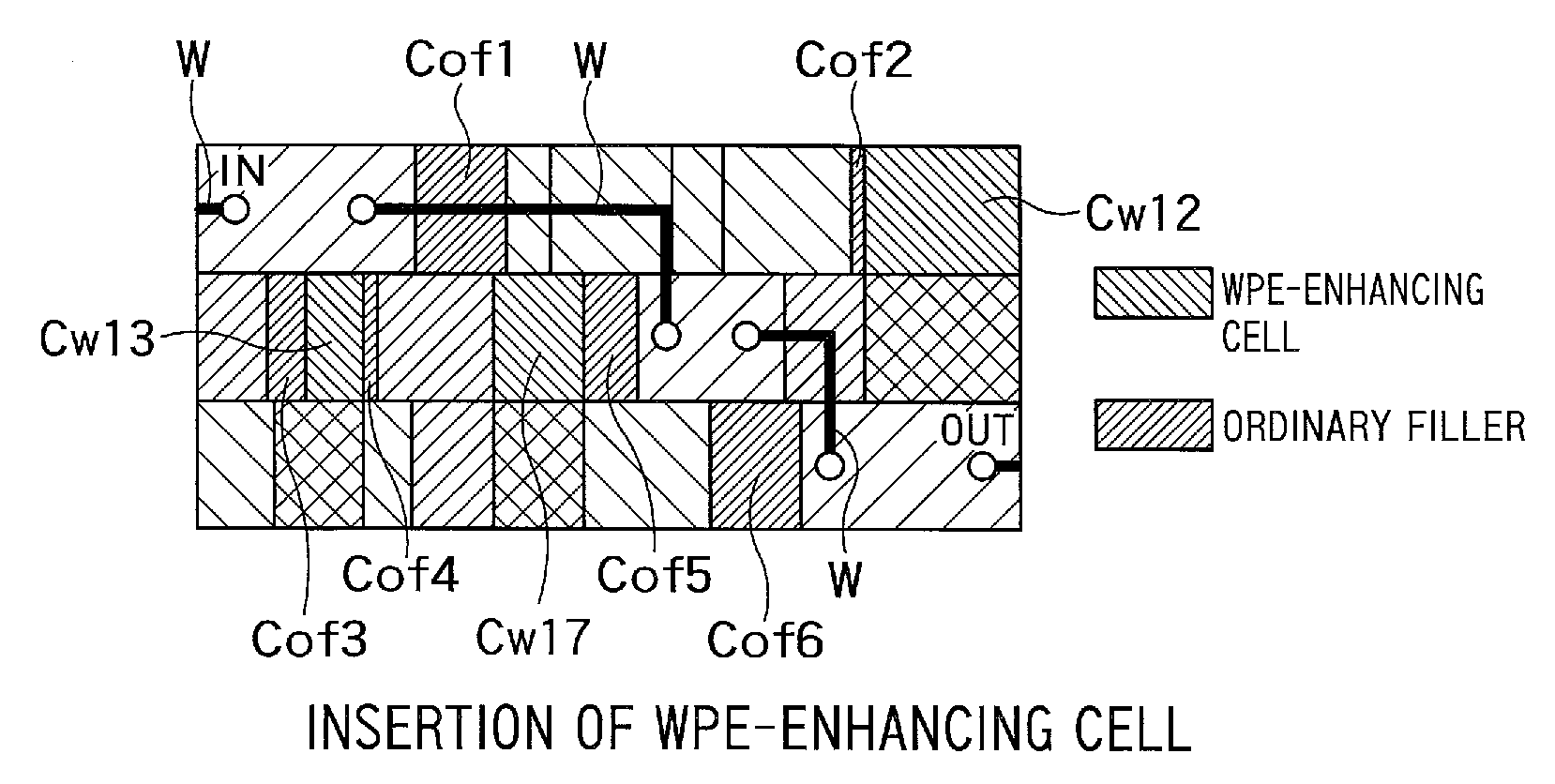
[0035]Hereafter, some of embodiments of the present invention will be described with reference to the drawings. In the drawings, identical reference numerals are given to identical components, and repetitive description on the identical components will be described only in case of necessity. It is to be noted that in the following description, the size of a standard cell in a carrier conduction direction in a MOSFET is referred to as a width of the standard cell and the size of a filler cell in the same direction is referred to as a width of the filler cell. Further, a direction perpendicular to the carrier conduction direction in the MOSFET, that is, a gate direction is referred to as a height direction. The size of the standard cell in the height direction is referred to as a height of the standard cell, and the size of a filler cell in the height direction is referred to as a height of the filler cell.

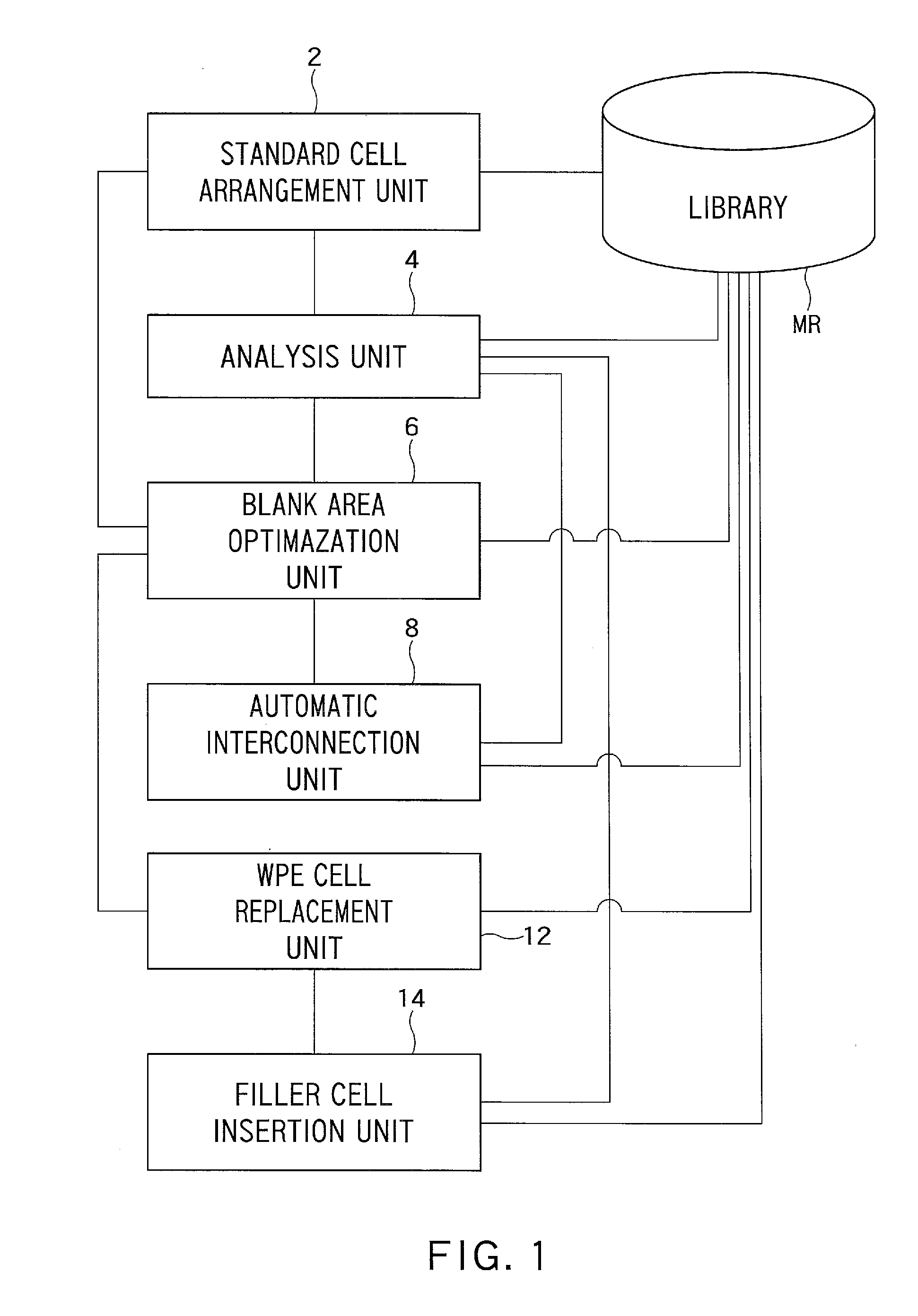
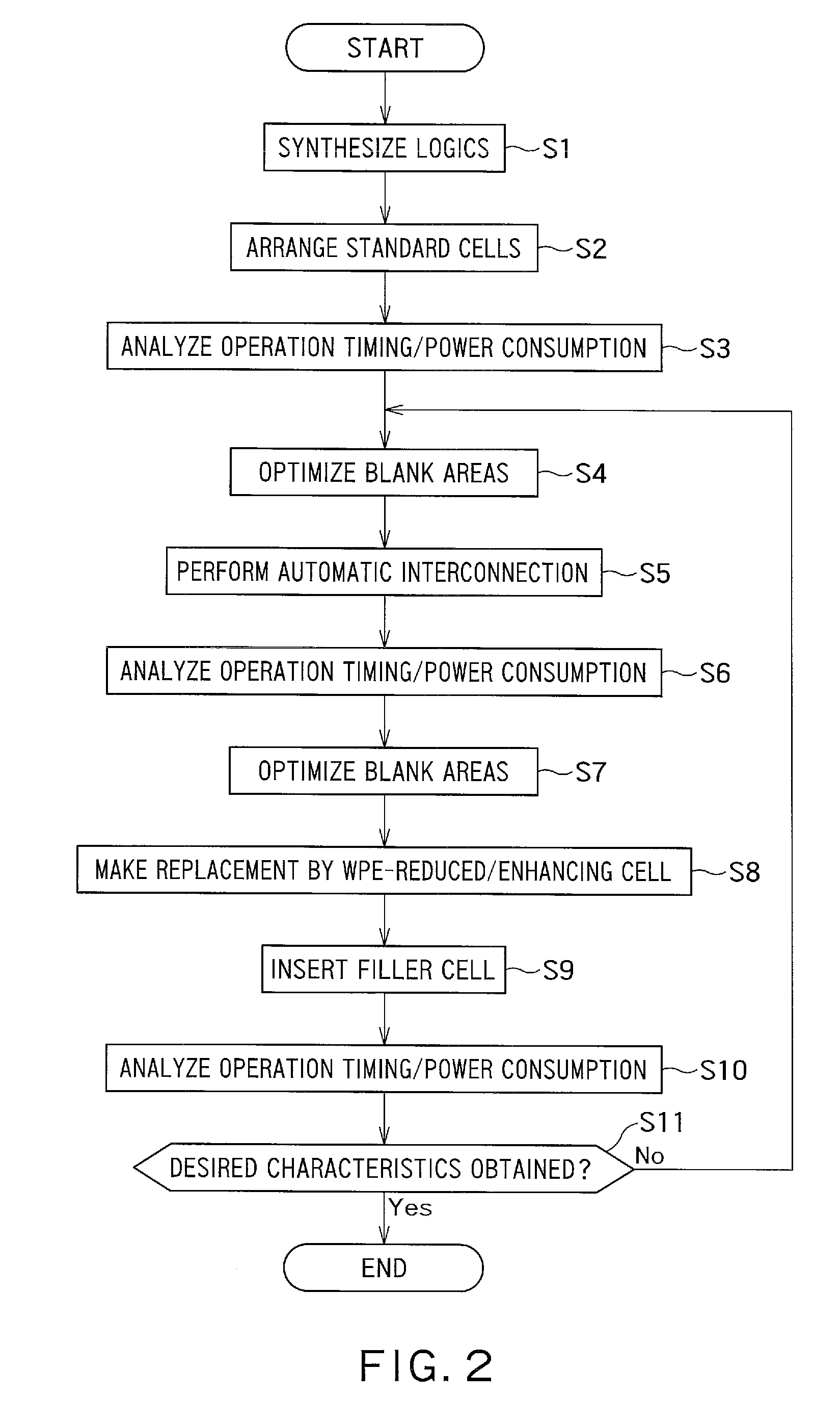
[0036]FIG. 1 is a block diagram showing the outlined constitution of a designin...


PUM


Abstract

A method of designing a semiconductor integrated circuit device includes: arranging standard cells constituting a MISFET; analyzing an operation timing and/or power consumption of the arranged standard cells; identifying one of the standard cells that is desired to have improved properties as a cell of interest based on the obtained analysis result; optimizing an arrangement and a shape of blank areas around the cell of interest taking into account an influence of a well proximity effect; and replacing the blank area and/or the cell of interest with a WPE-reduced or WPE-enhancing cell.

Description

CROSS REFERENCE TO RELATED APPLICATION[0001]This application claims benefit of priority under 35 USC §119 to Japanese patent application No. 2009-107604, filed on Apr. 27, 2009, the contents of which are incorporated by reference herein.BACKGROUND[0002]1. Field of the Invention[0003]The present invention relates to a semiconductor integrated circuit device and a method of designing the same.[0004]2. Related Background Art[0005]Recently, due to a desire for lowering power consumption, the power supply voltage of semiconductor devices has been reduced in general, which has raised a problem of increasing off-leakage currents. Thus, a method of solving such a problem is desired in designing a layout of the semiconductor integrated circuits.[0006]Further, as for a semiconductor integrated circuit device including metal insulator semiconductor field effect transistors (MISFETs), the problem of fluctuations in characteristics depending on the layout thereof is exposed according to the deve...

Claims


Application Information

Patent Timeline
IPC IPC(8): H01L29/78G06F17/50
CPCG06F17/5031G06F17/5072G06F2217/12H01L27/11807G06F2217/84H01L27/0207G06F2217/78G06F30/3312G06F30/392G06F2119/18G06F2119/06G06F2119/12Y02P90/02
Inventor INUKAI, TAKASHIKINOSHITA, KOICHIKANIE, MASATO
Owner KK TOSHIBA
Why Eureka
Try Eureka