Photoconductive switch package

Active Publication Date: 2010-11-11
LAWRENCE LIVERMORE NAT SECURITY LLC
View PDF21 Cites 22 Cited by
  • Summary
  • Abstract
  • Description
  • Claims
  • Application Information

AI Technical Summary

Benefits of technology

[0013]The invention is a photoconductive switch and method of making same. The switch is formed of a substrate that has a central portion of SiC or other photoconductive material and an outer portion of cvd-diamond or other suitable material surrounding the central portion. Conducting electrodes are formed on opposed sides of the substrate. The dimensions of the electrodes are greater than the dimensions of the cent

Problems solved by technology

The difficulty with these materials is that various failure mechanisms occur, even at modest parameters.
The principal issue with photoconductive switching has been short lifetime resulting from overstressing current and voltage conditions.
While promising, even SiC is subject to failure due to high electric fields locally produced where the electrodes separate from contact

Method used


Image

  • Photoconductive switch package
  • Photoconductive switch package
  • Photoconductive switch package

Examples


Embodiment Construction

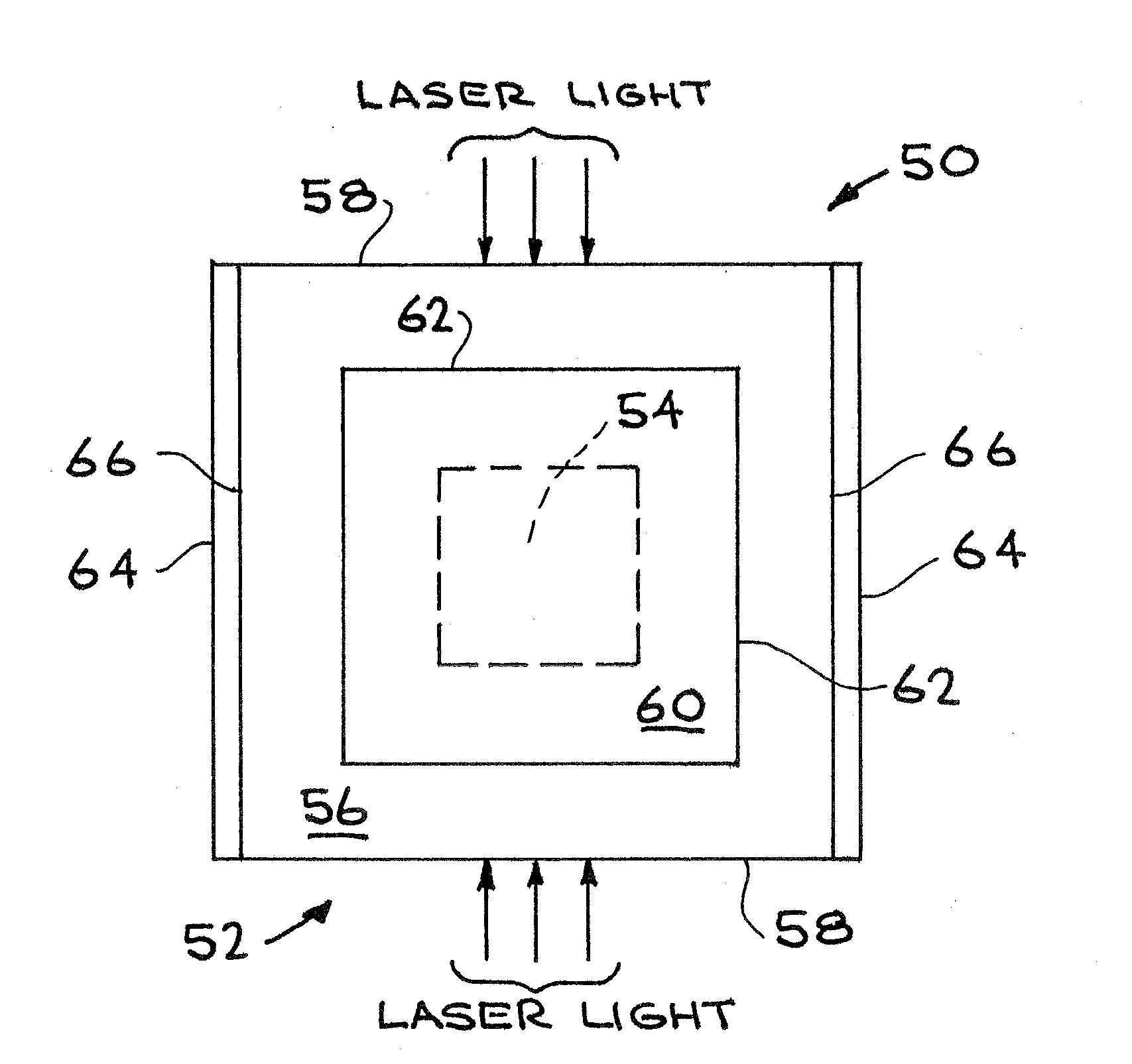
[0024]Referring more specifically to the drawings, for illustrative purposes the present invention is embodied in the apparatus and method generally shown in FIGS. 3A, B and 4. It will be appreciated that the apparatus may vary as to configuration and as to details of the parts, and the method may vary as to its particular implementation and as to specific steps and sequence, without departing from the basic concepts as disclosed herein.

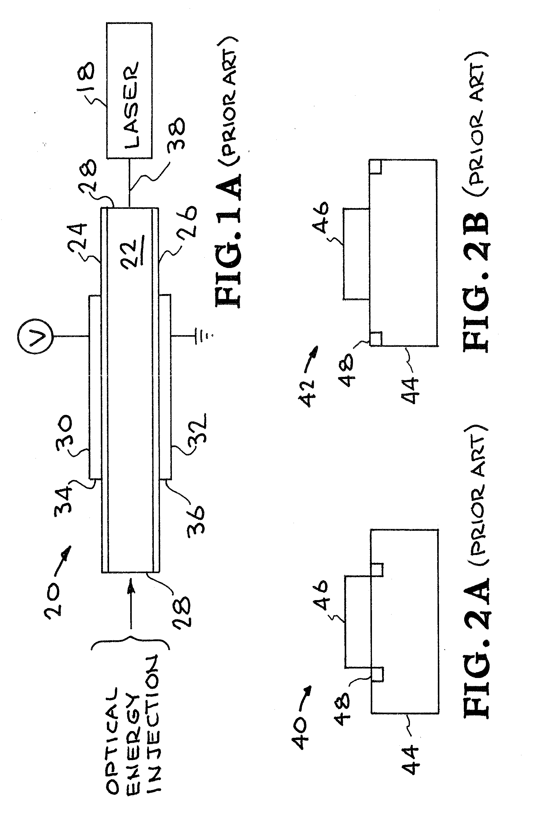
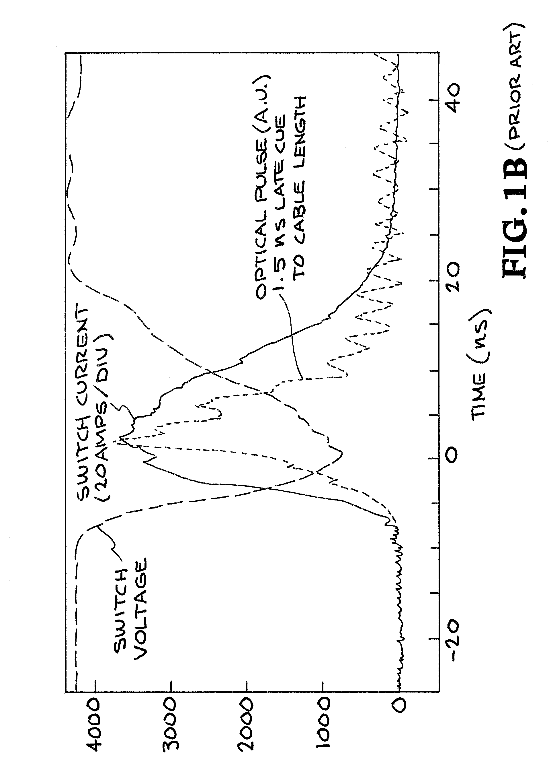
[0025]The photoconductive switch of the present invention is based on the basic prior art photoconductive switch construction and operation, with enhancements enabling the switch to handle high voltages and high currents with minimum inductance, rapid closure, precise temporal control and the possibility of long life. As such, the photoconductive switch of the present invention shares much the same construction and features as a basic photoconductive switch, generally having a substrate of photoconductive material between two electrodes. Without opti...


PUM

PropertyMeasurementUnit
Band gapaaaaaaaaaa
Electrical conductoraaaaaaaaaa
Electric potential / voltageaaaaaaaaaa

Abstract

A photoconductive switch is formed of a substrate that has a central portion of SiC or other photoconductive material and an outer portion of cvd-diamond or other suitable material surrounding the central portion. Conducting electrodes are formed on opposed sides of the substrate, with the electrodes extending beyond the central portion and the edges of the electrodes lying over the outer portion. Thus any high electric fields produced at the edges of the electrodes lie outside of and do not affect the central portion, which is the active switching element. Light is transmitted through the outer portion to the central portion to actuate the switch.

Description

RELATED APPLICATIONS[0001]This application claims priority from Provisional Application Ser. No. 61 / 176,375, filed May 7, 2009, titled “Photoconductive Switch Package” which is herein incorporated by reference.GOVERNMENT RIGHTS[0002]The United States Government has rights in this invention pursuant to Contract No. DE-AC52-07NA27344 between the United States Department of Energy and Lawrence Livermore National Security, LLC.BACKGROUND OF THE INVENTION[0003]1. Field of the Invention[0004]The present invention relates generally to photoconductive switches and more particularly to optically initiated silicon carbide (SiC) and other high voltage switches.[0005]2. Description of Related Art[0006]Particle accelerators, for example dielectric wall accelerators (DWAs), critically depend on high voltage, high current, fast closing switches that can be activated with nanosecond precision. Photoconductive switches offer the most potential in terms of handling such high voltages and high current...

Claims


Application Information

Patent Timeline
IPC IPC(8): H03K17/78H01H11/00
CPCH01L31/09Y10T29/49105H01L31/16
Inventor CAPORASO, GEORGE J.
Owner LAWRENCE LIVERMORE NAT SECURITY LLC
Why Eureka
Try Eureka