Method for producing layout of semiconductor integrated circuit with radio frequency devices
- Summary
- Abstract
- Description
- Claims
- Application Information
AI Technical Summary
Benefits of technology
Problems solved by technology
Method used
Image

Examples
Embodiment Construction
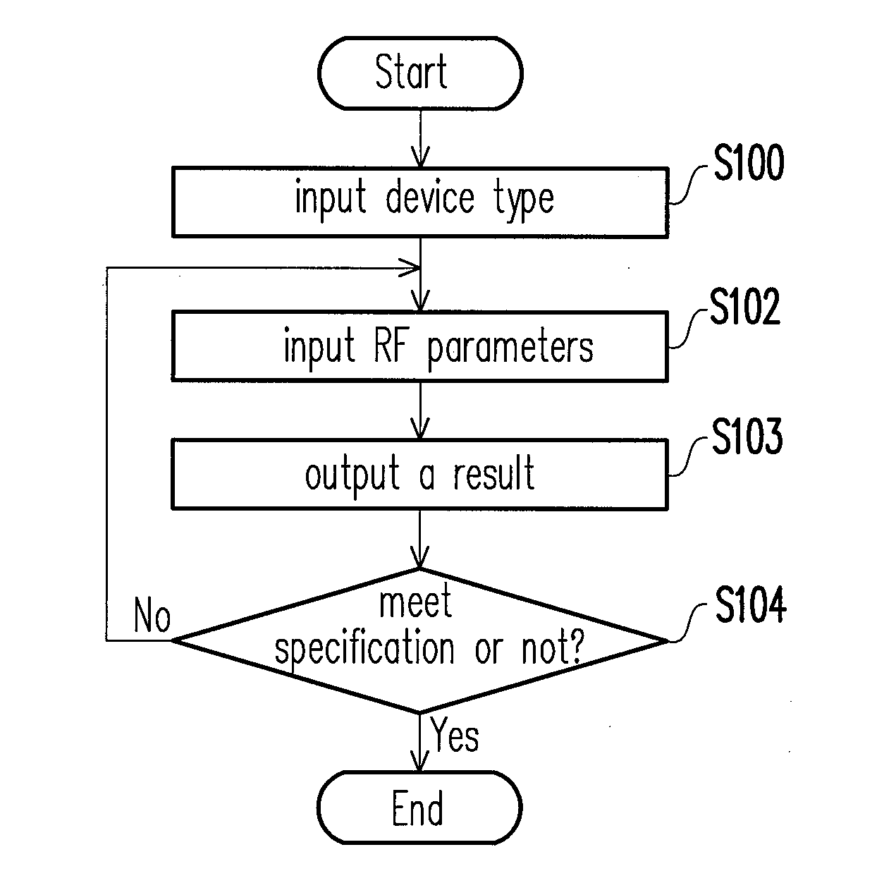
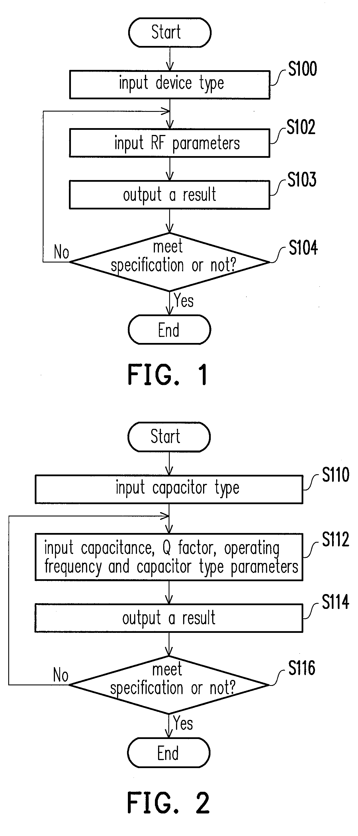
[0022]FIG. 1 is a schematic flow chart showing a layout method according to the embodiment of the present invention. First, in step S100, type information of at least one device is inputted. The device can be a capacitor device, an inductor device, a varactor device, a transformer device, or resistor and a transistor working under RF range. As for the type information of a device, the type information of the capacitor device can be stacked type information of multiple metal layers. The type information of an inductor device can be a shape of the inductor.
[0023]In step S102, after a device and required type information are inputted, at least one RF parameter corresponding to the device is inputted. The RF parameter can be an operating frequency and a corresponding Q factor. Besides, considering a frequency response of the device under the radio frequency, a value of the device itself is quite important. For example, a capacitance, an inductance, a resistance are required to be inputt...
PUM
 Abstract
Description
Claims
Application Information