Eureka AIR delivers breakthrough ideas for toughest innovation challenges, trusted by R&D personnel around the world.

Method for producing layout of semiconductor integrated circuit with radio frequency devices

a radio frequency device and integrated circuit technology, applied in computer aided design, electrical equipment, transmission, etc., can solve the problems of inability to change the layout design, the redesign or the change of the layout design is undesired, and the layout design is generally taken a lot of time, so as to achieve efficient and time-saving methods

Inactive Publication Date: 2008-08-21
UNITED MICROELECTRONICS CORP
View PDF9 Cites 21 Cited by
  • Summary
  • Abstract
  • Description
  • Claims
  • Application Information

AI Technical Summary

Benefits of technology

[0008]In view of the above, the present invention is to provide an efficient and time-saving method for producing a layout of an IC with RF devices.
[0014]Through the above-mentioned embodiments, time for designers to design the layout diagram can be reduced. Through inputting the parameter of the RF device such as the operating frequency, the Q factor, and the area, the optimized device dimension and the layout design can be obtained.

Problems solved by technology

However, due to the above concern of the optimization of the area, most IC layout designers at the current stage do not take the IC layout design into consideration as the RF devices e.g. a capacitor, an inductor, and a varactor are included in the IC chip.
Taking a capacitor for example, designing with a pre-simulation or a post-simulation takes too much time.
However, from the viewpoint of efficiency and smart layout design, either the redesign or the change of the layout design is undesired.
However, the EM simulation is generally taking a lot of time.

Method used


Image

  • Method for producing layout of semiconductor integrated circuit with radio frequency devices
  • Method for producing layout of semiconductor integrated circuit with radio frequency devices
  • Method for producing layout of semiconductor integrated circuit with radio frequency devices

Examples


Embodiment Construction

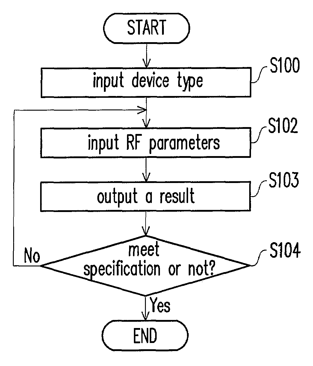
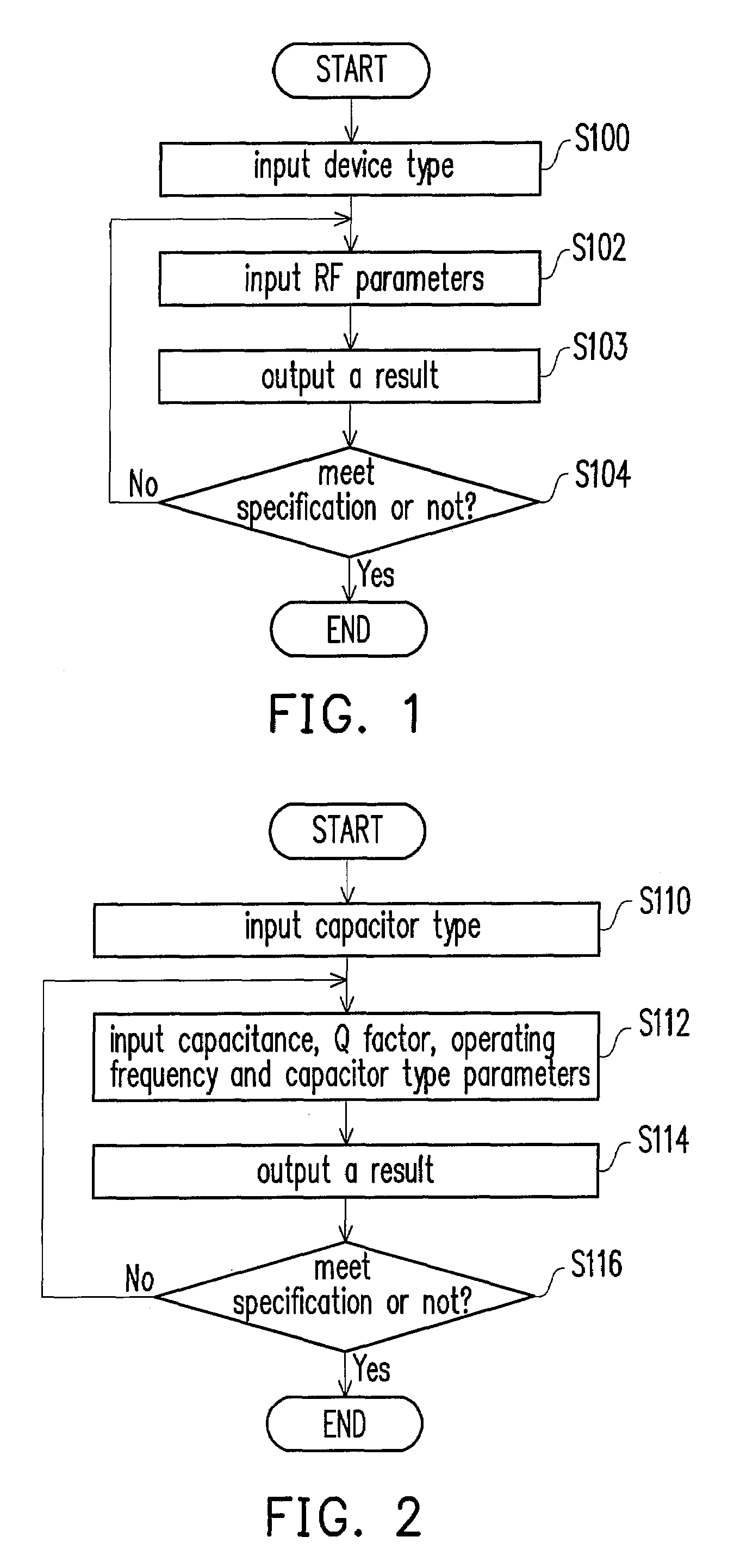
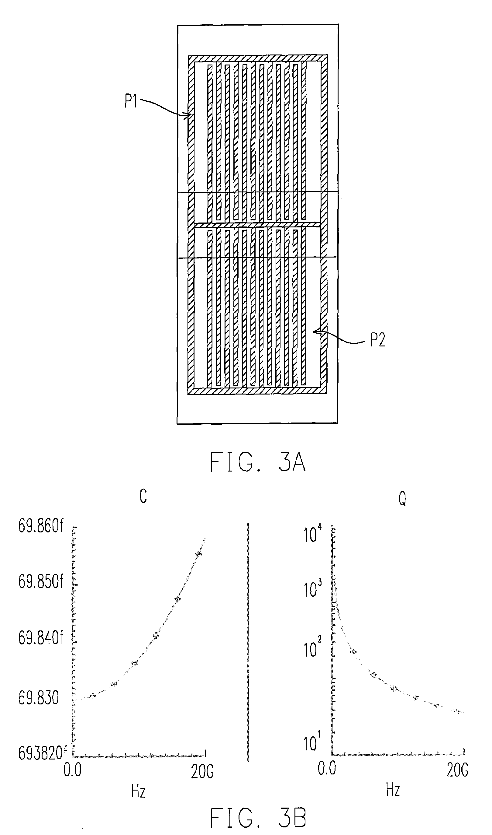
[0025]FIG. 1 is a schematic flow chart showing a layout method according to the embodiment of the present invention. First, in step S100, type information of at least one device is inputted. The device can be a capacitor device, an inductor device, a varactor device, a transformer device, or resistor and a transistor working under RF range. As for the type information of a device, the type information of the capacitor device can be stacked type information of multiple metal layers. The type information of an inductor device can be a shape of the inductor.

[0026]In step S102, after a device and required type information are inputted, at least one RF parameter corresponding to the device is inputted. The RF parameter can be an operating frequency and a corresponding Q factor. Besides, considering a frequency response of the device under the radio frequency, a value of the device itself is quite important. For example, a capacitance, an inductance, a resistance are required to be inputt...


PUM


Abstract

A method for producing an IC layout with radio frequency devices is provided. The method has following steps. Type information of at least one RF device is inputted, and at least one RF parameter corresponding to the RF device is inputted as well. A frequency response result is then generated based on the type information and the RF parameter. When the frequency response result meets the required specification, an IC layout process is performed based on the frequency response result. However, when the frequency response result doesn't meet the required specification, another RE parameter is inputted again to produce new frequency response result.

Description

BACKGROUND OF THE INVENTION[0001]1. Field of the Invention[0002]The present invention relates to a method for producing a layout of an integrated circuit (IC), and more particularly to a method for producing a layout of an integrated circuit (IC) with radio frequency (RF) devices.[0003]2. Description of Related Art[0004]An IC layout plays an important role in producing an integrated circuit. With the demand of reducing an IC size, it is significant to dispose most devices in a limited area and meet required specifications. However, due to the above concern of the optimization of the area, most IC layout designers at the current stage do not take the IC layout design into consideration as the RF devices e.g. a capacitor, an inductor, and a varactor are included in the IC chip.[0005]Taking a capacitor for example, designing with a pre-simulation or a post-simulation takes too much time. If the required specifications are not satisfied, a re-design or a change of the layout design is n...

Claims


Application Information

Patent Timeline
IPC IPC(8): H04B1/44
CPCG06F17/5063G06F30/36
Inventor HSU, TSUN-LAICHEN, JUI-FANGOU, JUN-HONGHSU, JI-WEI
Owner UNITED MICROELECTRONICS CORP
Why Eureka
Eureka Blog
Learn More