Power semiconductor module

Active Publication Date: 2011-03-17
MITSUBISHI ELECTRIC CORP
View PDF8 Cites 40 Cited by
  • Summary
  • Abstract
  • Description
  • Claims
  • Application Information

AI Technical Summary

Benefits of technology

[0011]According to the present invention, when the switching element included in the first semiconductor element is switched, a surge current flows through the second semiconductor elements located at both sides. In contrast, when the switching element included in the second semiconductor element is switched, a surge current f

Problems solved by technology

The area of the semiconductor element is increased in proportion to the withstand voltage, leading to increase in the size and cost of the module.
Moreover, EMI (Electromagnetic Magnetic Interference) will be generated externally if the surge voltage is

Method used


Image

  • Power semiconductor module
  • Power semiconductor module
  • Power semiconductor module

Examples


first embodiment

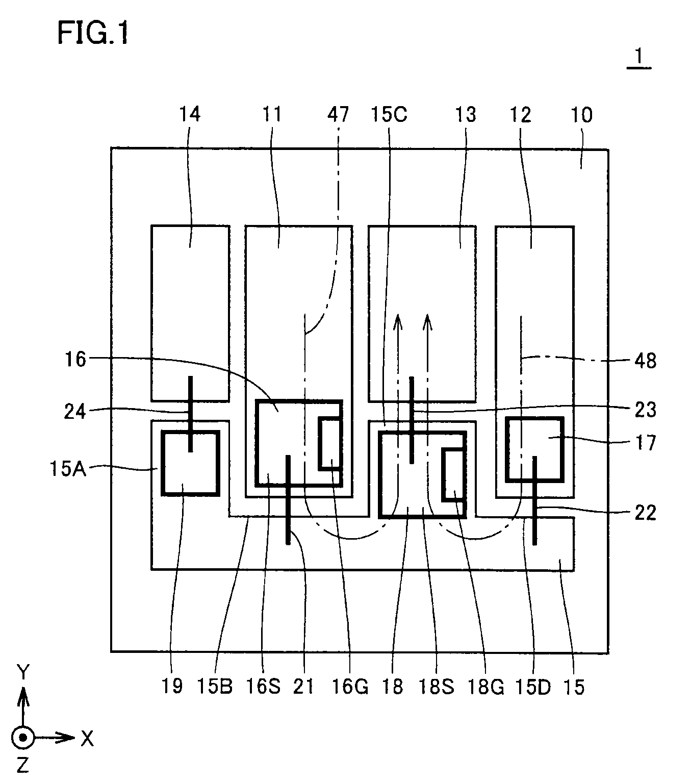
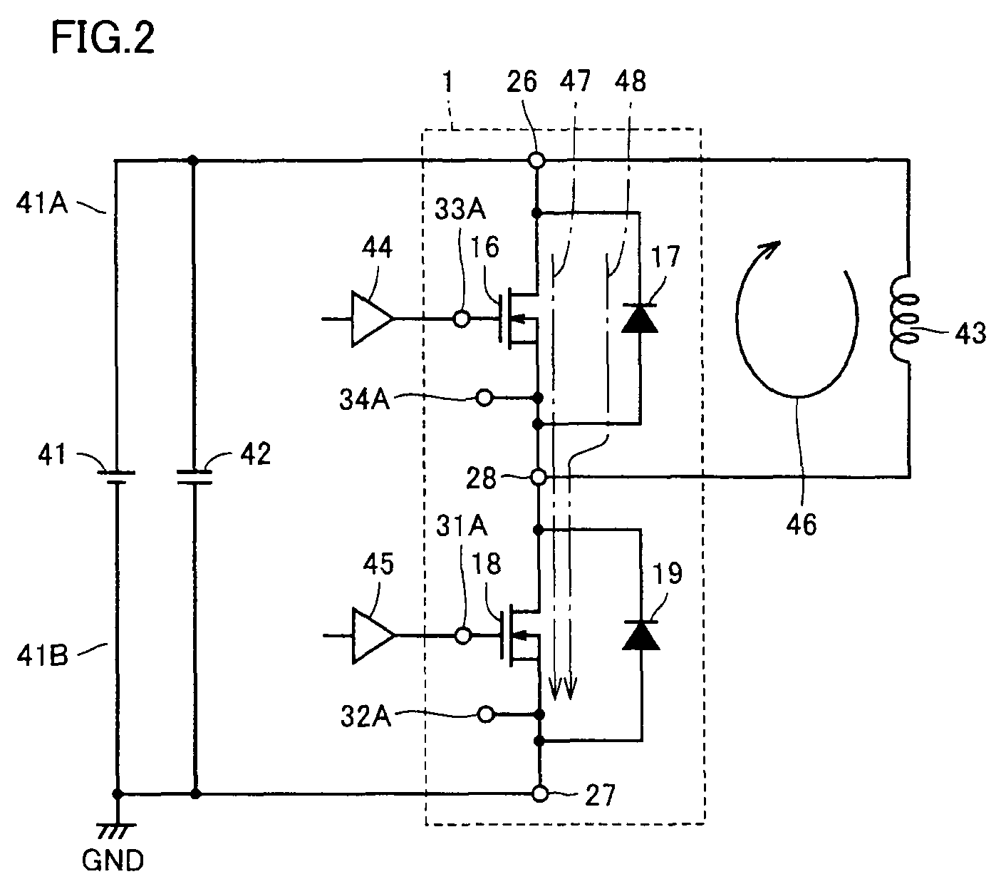
[0022]FIG. 1 is a plan view showing a configuration of the main part of a power semiconductor module 1 according to a first embodiment of the present invention. In FIG. 1, the lateral direction, the vertical direction, and the direction perpendicular to the drawing sheet are taken as the X direction, the Y direction and the Z direction, respectively. The direction from the left side towards the right side in the drawing is the +X direction. The direction from the lower side towards the upper side in the drawing is the +Y direction. The direction from the back side to the top side of the drawing sheet is the +Z direction. An insulation substrate 10 shown in FIG. 1 is arranged along the XY plane. The thickness direction of insulation substrate 10 corresponds to the Z direction. FIG. 1 represents the state prior to coupling a P side power supply terminal 26, an N side power supply terminal 27, and a load side output terminal 28 to insulation substrate 10. The arrangement of these termi...

second embodiment

[0067]FIG. 6 is a plan view showing a configuration of the main part of a power semiconductor module 2 according to a second embodiment of the present invention. In FIG. 6, the lateral direction, the vertical direction, and the direction perpendicular to the drawing sheet are taken as the X direction, the Y direction and the Z direction, respectively. The direction from the left side towards the right side in the drawing is the +X direction. The direction from the lower side towards the upper side in the drawing is the +Y direction. The direction from the back side to the top side of the drawing sheet is the +Z direction. An insulation substrate 10 shown in FIG. 6 is arranged along the XY plane. The thickness direction of insulation substrate 10 corresponds to the Z direction.

[0068]FIG. 7 is a circuit diagram corresponding to power semiconductor module 2 of FIG. 6.

[0069]Referring to FIGS. 6 and 7, power semiconductor module 2 takes a configuration in which a plurality (three) of pow...

third embodiment

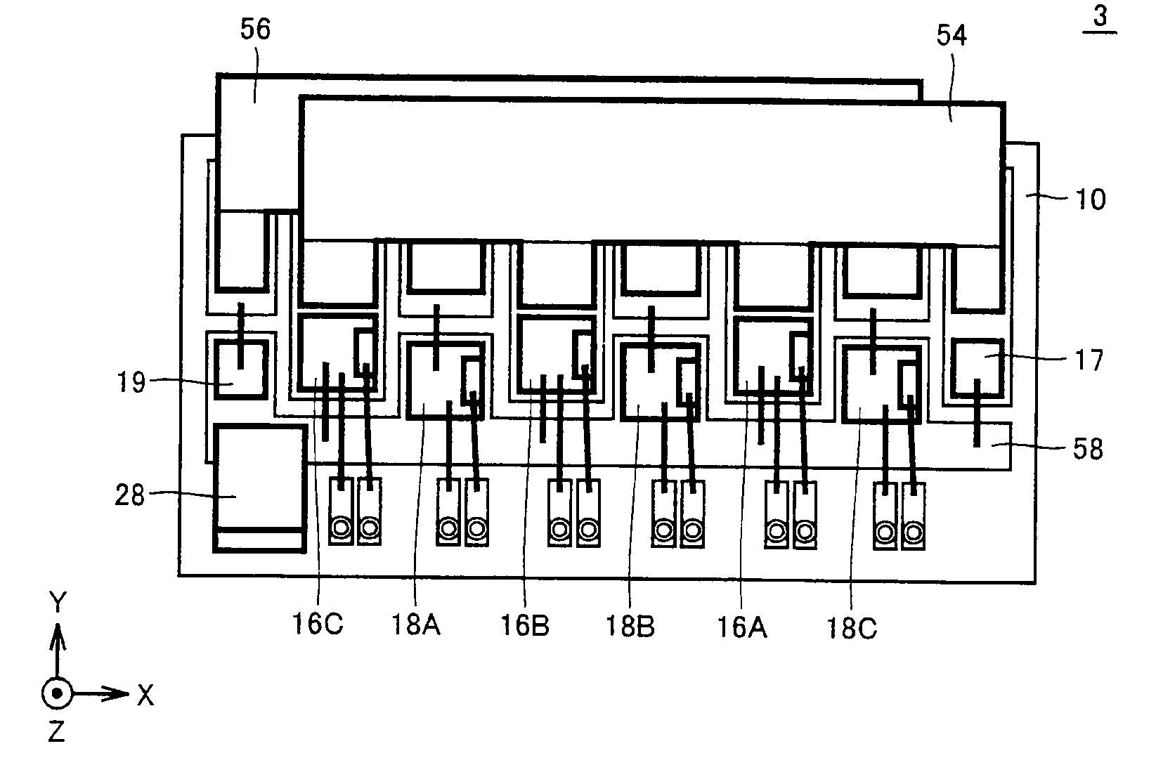
[0072]FIG. 8 is a plan view showing a configuration of the main part of a power semiconductor module 3 according to a third embodiment of the present invention. In FIG. 8, the lateral direction, the vertical direction, and the direction perpendicular to the drawing sheet are taken as the X direction, the Y direction and the Z direction, respectively. The direction from the left side towards the right side in the drawing is the +X direction. The direction from the lower side towards the upper side in the drawing is the +Y direction. The direction from the back side to the top side of the drawing sheet is the +Z direction. An insulation substrate 10 shown in FIG. 8 is arranged along the XY plane. The thickness direction of insulation substrate 10 corresponds to the Z direction.

[0073]FIG. 9 is a circuit diagram corresponding to power semiconductor module 3 of FIG. 7.

[0074]Referring to FIGS. 8 and 9, power semiconductor module 3 is configured having two MOS transistors added parallel to...


PUM


Abstract

A power semiconductor module (1) includes a first MOS transistor (16) connected to a positive side power supply terminal via a first conductor pattern (11), a first free wheeling diode (17) connected to the positive side power supply terminal via a second conductor pattern (12), a second MOS transistor (18) connected to a negative side power supply terminal via a third conductor pattern (13), and a second free wheeling diode (19) connected to the negative side power supply terminal via a fourth conductor pattern (14). These semiconductor elements (16-19) are connected to a load side output terminal via a common fifth conductor pattern (15). The semiconductor element (16, 17) connected to the positive side power supply terminal and the semiconductor element (18, 19) connected to the negative side power supply terminal are arranged alternately, substantially linearly.

Description

TECHNICAL FIELD[0001]The present invention relates to a power semiconductor module including a semiconductor switching element and diode for electric power.BACKGROUND ART[0002]A power semiconductor module has a problem in suppressing a surge voltage that is generated when a semiconductor switching element is switched. Therefore, it is necessary to reduce the wiring inductance.[0003]For example, Japanese Patent Laying-Open No. 2005-216876 (Patent Document 1) relates to a power semiconductor module configuring upper and lower arms of one phase by connecting in series two of a group of elements for one arm, each group formed of an IGBT (Insulated Gate Bipolar Transistor) chip and a diode chip connected antiparallel to the IGBT. The input / output terminal of the IGBT is connected to positive side DC power supply terminal, a negative side DC power supply terminal, and a load side output terminal via a copper foil pattern insulated from each other on an insulative substrate. The wire corre...

Claims


Application Information

Patent Timeline
IPC IPC(8): H01L29/68
CPCH01L23/552H01L25/072H01L25/18H01L2924/13091H01L2224/0603H01L2924/12032H01L2924/13055H01L2224/48227H01L2924/1305H01L2924/30107H01L2924/00H01L2924/1301H01L25/07
Inventor NAKATA, SHUHEI
Owner MITSUBISHI ELECTRIC CORP
Why Eureka
Try Eureka