

Power semiconductor module
a technology of semiconductor modules and semiconductors, applied in the direction of semiconductor devices, semiconductor/solid-state device details, electrical apparatus, etc., can solve the problems erroneous operation of external devices, increasing the size and cost of modules, etc., and achieve the effect of reducing the wiring inductan
- Summary
- Abstract
- Description
- Claims
- Application Information
AI Technical Summary
Benefits of technology
Problems solved by technology
Method used
Image

Examples
first embodiment
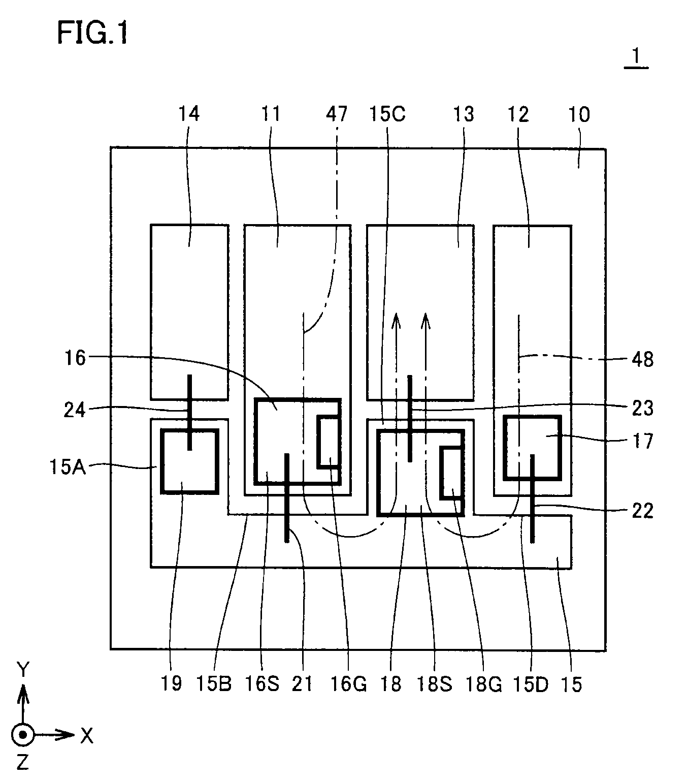
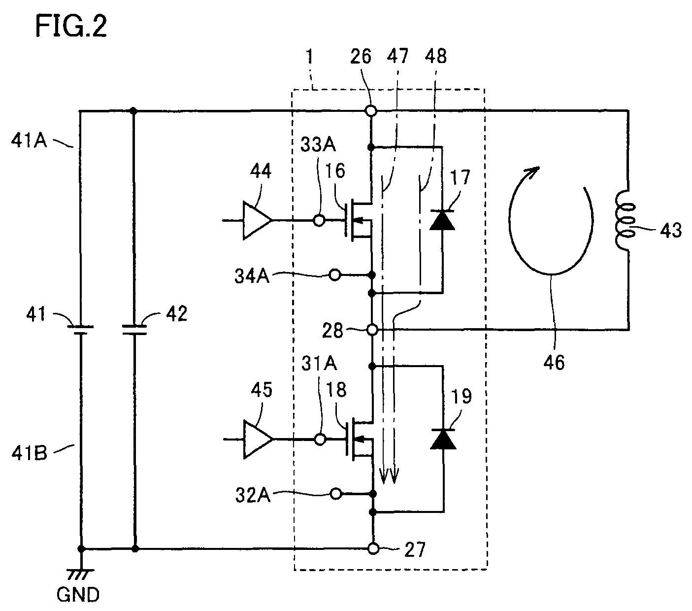
[0022]FIG. 1 is a plan view showing a configuration of the main part of a power semiconductor module 1 according to a first embodiment of the present invention. In FIG. 1, the lateral direction, the vertical direction, and the direction perpendicular to the drawing sheet are taken as the X direction, the Y direction and the Z direction, respectively. The direction from the left side towards the right side in the drawing is the +X direction. The direction from the lower side towards the upper side in the drawing is the +Y direction. The direction from the back side to the top side of the drawing sheet is the +Z direction. An insulation substrate 10 shown in FIG. 1 is arranged along the XY plane. The thickness direction of insulation substrate 10 corresponds to the Z direction. FIG. 1 represents the state prior to coupling a P side power supply terminal 26, an N side power supply terminal 27, and a load side output terminal 28 to insulation substrate 10. The arrangement of these termi...
second embodiment
[0067]FIG. 6 is a plan view showing a configuration of the main part of a power semiconductor module 2 according to a second embodiment of the present invention. In FIG. 6, the lateral direction, the vertical direction, and the direction perpendicular to the drawing sheet are taken as the X direction, the Y direction and the Z direction, respectively. The direction from the left side towards the right side in the drawing is the +X direction. The direction from the lower side towards the upper side in the drawing is the +Y direction. The direction from the back side to the top side of the drawing sheet is the +Z direction. An insulation substrate 10 shown in FIG. 6 is arranged along the XY plane. The thickness direction of insulation substrate 10 corresponds to the Z direction.
[0068]FIG. 7 is a circuit diagram corresponding to power semiconductor module 2 of FIG. 6.
[0069]Referring to FIGS. 6 and 7, power semiconductor module 2 takes a configuration in which a plurality (three) of pow...
third embodiment
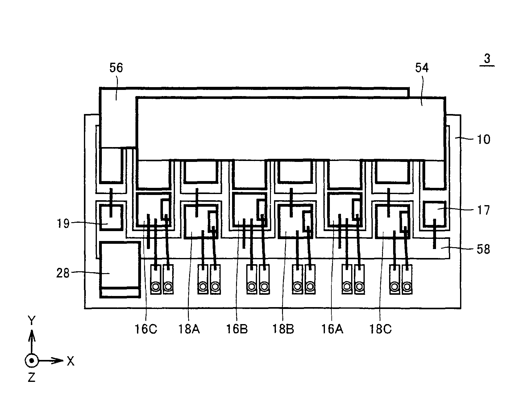
[0072]FIG. 8 is a plan view showing a configuration of the main part of a power semiconductor module 3 according to a third embodiment of the present invention. In FIG. 8, the lateral direction, the vertical direction, and the direction perpendicular to the drawing sheet are taken as the X direction, the Y direction and the Z direction, respectively. The direction from the left side towards the right side in the drawing is the +X direction. The direction from the lower side towards the upper side in the drawing is the +Y direction. The direction from the back side to the top side of the drawing sheet is the +Z direction. An insulation substrate 10 shown in FIG. 8 is arranged along the XY plane. The thickness direction of insulation substrate 10 corresponds to the Z direction.
[0073]FIG. 9 is a circuit diagram corresponding to power semiconductor module 3 of FIG. 7.
[0074]Referring to FIGS. 8 and 9, power semiconductor module 3 is configured having two MOS transistors added parallel to...
PUM
 Abstract
Description
Claims
Application Information