Unlock instant, AI-driven research and patent intelligence for your innovation.
Integrated circuit packaging system with package-on-package and method of manufacture thereof
Active Publication Date: 2011-03-17
STATS CHIPPAC LTD
View PDF17 Cites 29 Cited by
Summary
Abstract
Description
Claims
Application Information
AI Technical Summary
This helps you quickly interpret patents by identifying the three key elements:
Problems solved by technology
Method used
Benefits of technology
Problems solved by technology
However, despite these several reductions in size, IC density continues to be limited by the space or “real estate” available for mounting chips on a substrate.
Unfortunately, limitations of current PoP packing techniques can interfere with the ready incorporation and utilization of existing die and package configurations.
It can also interfere with and limit the development of necessary increases in the input / output (“I / O”) connections that are needed and that need to be accommodated within such PoP packages as they grow ever more complex with ever increasing functionality and capability.
Solutions to these problems have been long sought but prior developments have not taught or suggested any solutions and, thus, solutions to these problems have long eluded those skilled in the art.
Method used
Image
Click on the blue label to locate the original text in one second.
Reading with bidirectional positioning of images and text.
Examples
first embodiment
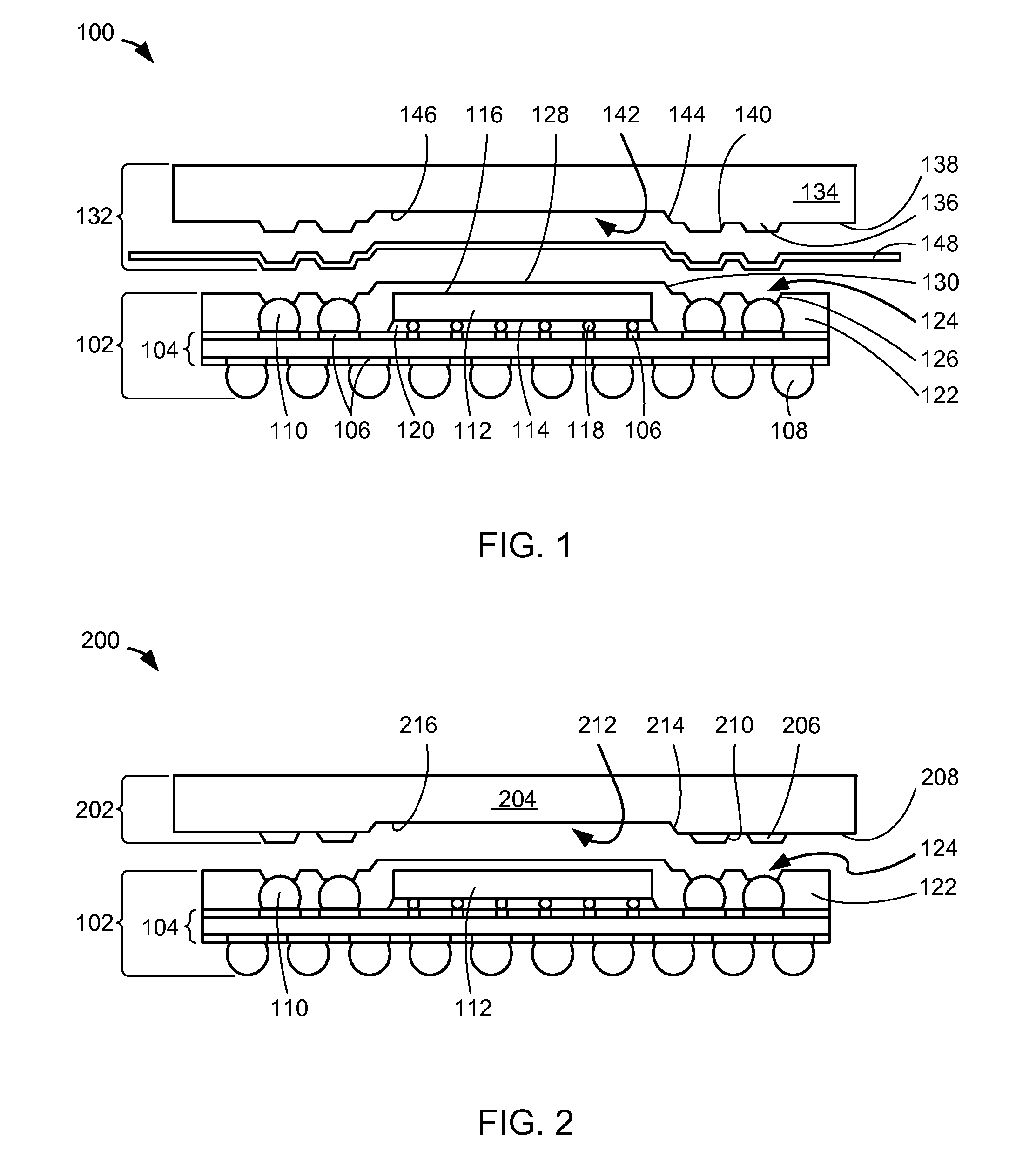
[0028]Referring now to FIG. 1, therein is shown a cross-sectional view of an integrated circuit packaging system 100 along a section line 1-1 of FIG. 3 in the present invention. The integrated circuit packaging system 100 can include a base integrated circuit package 102.
[0029]The base integrated circuit package 102 can include a base substrate 104, such as a printed circuit board (PCB), a laminated plastic substrate, a laminated ceramic substrate, or a carrier. The base substrate 104 can include a base substrate pad 106, such as an electrical contact or a contact pad, for providing electrical connection to the base substrate 104. The base substrate pad 106 can include any planar dimension.
[0030]The base integrated circuit package 102 can include an external interconnect 108, such as a solder ball or a solder bump, for providing electrical connectivity to external systems. The external interconnect 108 can be attached to the base substrate pad 106. The external interconnect 108 can ...
second embodiment
[0051]Referring now to FIG. 2, therein is shown a cross-sectional view similar to FIG. 1 of an integrated circuit packaging system 200 in the present invention. The integrated circuit packaging system 200 can include the base integrated circuit package 102.
[0052]The integrated circuit packaging system 200 can include an encapsulation system 202 for forming the base encapsulation 122. The encapsulation system 202 can include a mold chase 204, such as a top mold chase, a top gate mold chase, or a lateral gate mold chase. The mold chase 204 can be secured, engaged, or joined to the base integrated circuit package 102.
[0053]The mold chase 204 can include a buffer layer 206, such as an elastomer, a silicone rubber, a heat-resistance plastic or rubber, a polyimide or fluorinated resin, an elastic material, or a soft material. The buffer layer 206 can be attached to a first bottom surface 208 of the mold chase 204. The buffer layer 206 can be provided for forming an area array of the reces...
third embodiment
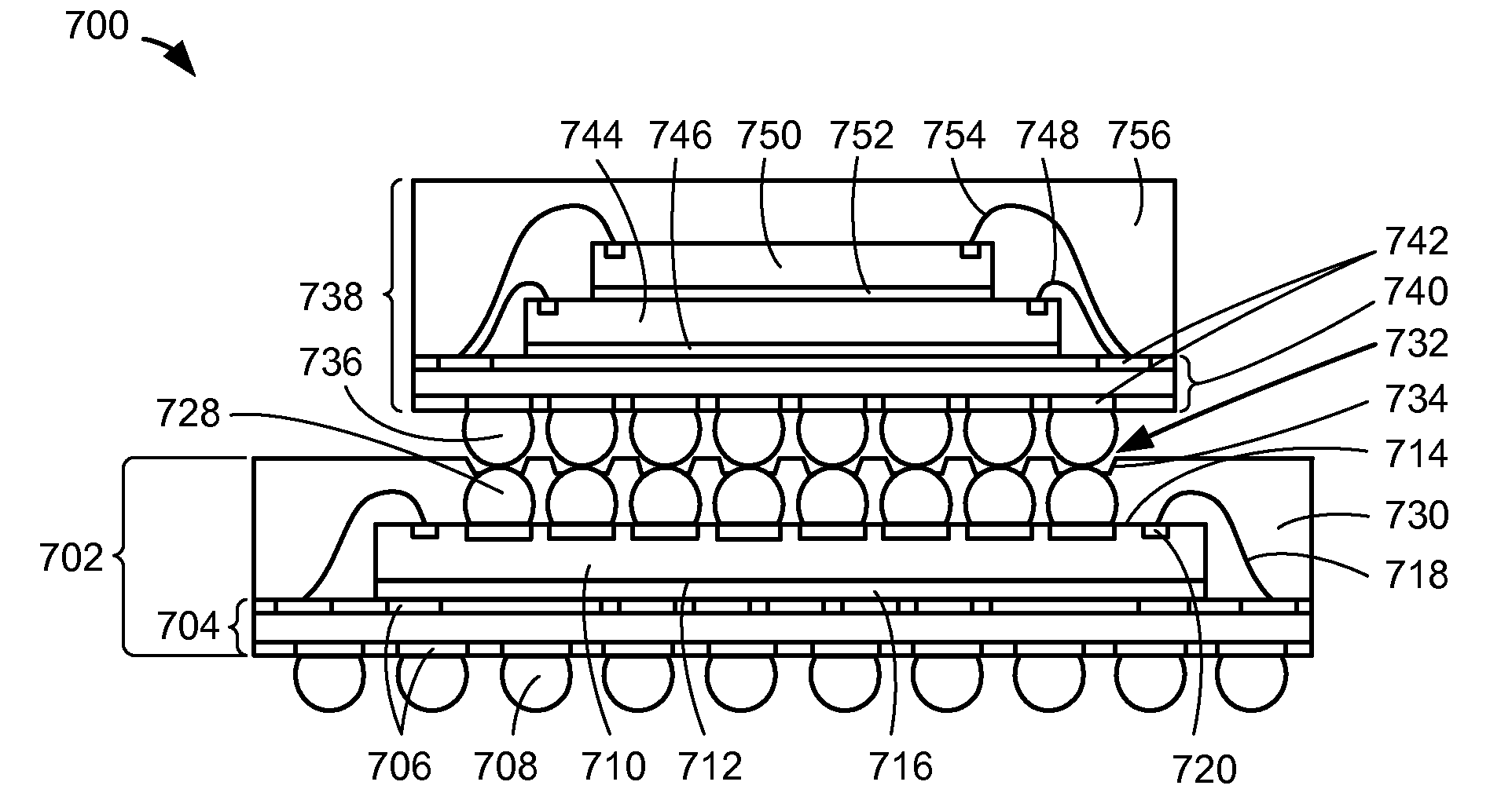
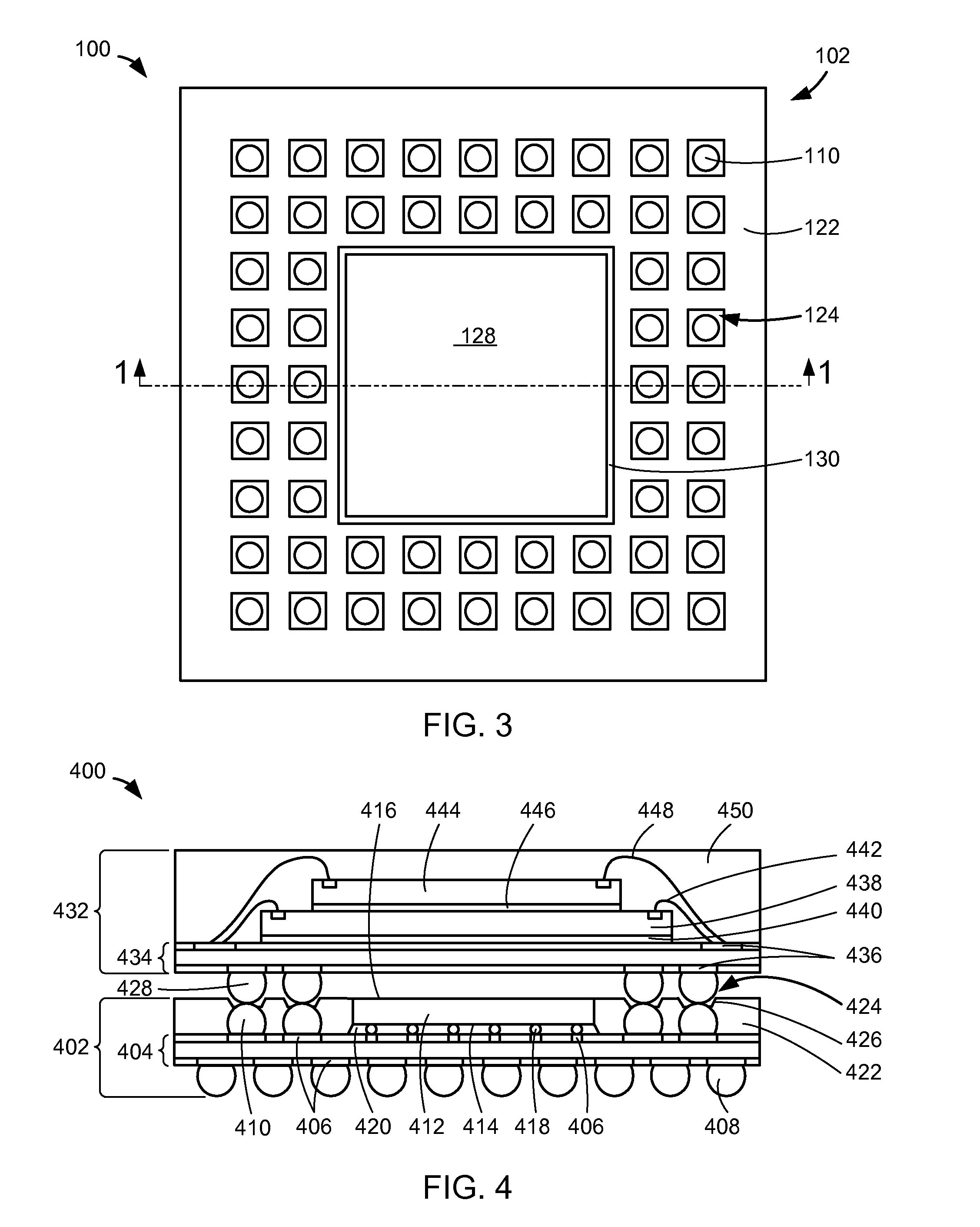
[0062]Referring now to FIG. 4, therein is shown a cross-sectional view of an integrated circuit packaging system 400 along a section line 4-4 of FIG. 5 in the present invention. The integrated circuit packaging system 400 can include a base integrated circuit package 402.
[0063]The base integrated circuit package 402 can include a base substrate 404, such as a printed circuit board (PCB), a laminated plastic substrate, a laminated ceramic substrate, or a carrier. The base substrate 404 can include a base substrate pad 406, such as an electrical contact or a contact pad, for providing electrical connection to the base substrate 404. The base substrate pad 406 can include any planar dimension.
[0064]The base integrated circuit package 402 can include an external interconnect 408, such as a solder ball or a solder bump, for providing electrical connectivity to external systems. The external interconnect 408 can be attached to the base substrate pad 406. The external interconnect 408 can ...
PUM
Abstract
A method of manufacture of an integrated circuit packaging system includes: providing an encapsulation system having a mold chase with a buffer layer attached thereto; forming a base integrated circuitpackage including: providing a base substrate, connecting an exposed interconnect to the base substrate, a portion of the exposed interconnect having the buffer layer attached thereon, mounting a base component over the base substrate, forming a base encapsulation over the base substrate and the exposed interconnect using the encapsulation system; and releasing the encapsulation system providing the portion of the exposed interconnect exposed from the base encapsulation, the exposed interconnect having characteristics of the buffer layer removed.
Description
TECHNICAL FIELD[0001]The present invention relates generally to an integrated circuit packaging system, and more particularly to a system for an integrated circuit packaging system with package-on-package.BACKGROUND ART[0002]Important and constant goals of the computer industry include higher performance, lower cost, increased miniaturization of components, and greater packaging density for integrated circuits (“ICs”). As new generations of IC products are released, the number of IC devices needed to fabricate them tends to decrease due to advances in technology. Simultaneously, the functionality of these IC products increases. For example, on the average there is approximately a 10 percent decrease in components required for every IC product generation over a previous generation having equivalent functionality.[0003]Semiconductor package structures continue to become thinner and ever more miniaturized. This results in increased component density in semiconductor packages and decrea...
Claims
Application Information
Patent Timeline
Application Date:The date an application was filed.
Publication Date:The date a patent or application was officially published.
First Publication Date:The earliest publication date of a patent with the same application number.
Issue Date:Publication date of the patent grant document.
PCT Entry Date:The Entry date of PCT National Phase.
Estimated Expiry Date:The statutory expiry date of a patent right according to the Patent Law, and it is the longest term of protection that the patent right can achieve without the termination of the patent right due to other reasons(Term extension factor has been taken into account ).
Invalid Date:Actual expiry date is based on effective date or publication date of legal transaction data of invalid patent.