Method of driving plasma display panel, and plasma display apparatus

a technology of plasma display panel and plasma display apparatus, which is applied in the direction of instruments, computing, electric digital data processing, etc., can solve the problems of performance difference and degradation of the display quality of the plasma display panel

Inactive Publication Date: 2011-06-09
PANASONIC CORP
View PDF2 Cites 2 Cited by
  • Summary
  • Abstract
  • Description
  • Claims
  • Application Information

AI Technical Summary

Benefits of technology

[0043]In accordance with the present invention, it is possible to provide a driving method of a plasma display panel in which a sufficient sub-field number is ensured even in a high-definition plasma display panel, and a luminance difference is less likely to be generated in the vicinity of a display region which is a boundary between display electrode pair groups, and a plasma display apparatus using the driving method.

Problems solved by technology

This results in a degraded display quality of the plasma display panel.
Furthermore, if the luminance difference is increased if a performance difference between the plural scan electrode driving circuits and a performance difference between the plural sustain electrode driving circuits, are significant.

Method used


Image

  • Method of driving plasma display panel, and plasma display apparatus
  • Method of driving plasma display panel, and plasma display apparatus
  • Method of driving plasma display panel, and plasma display apparatus

Examples


embodiment 1

[0058]10>

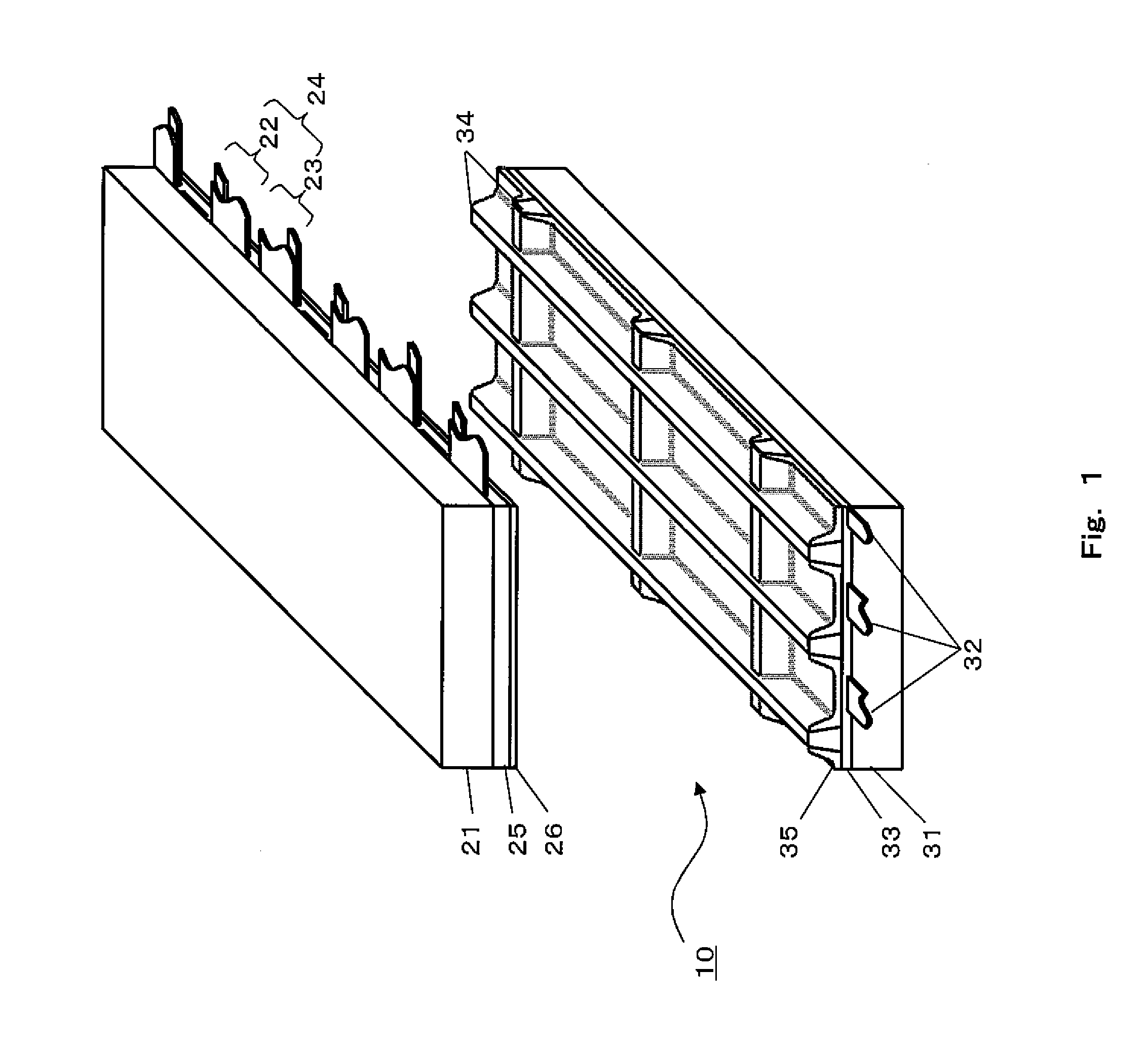
[0059]FIG. 1 is an exploded perspective view of a plasma display panel 10 of a plasma display apparatus according to Embodiment 1 of the present invention. Plural display electrode pairs 24 each including a scan electrode 22 and a sustain electrode 23 are formed on a glass-made front substrate 21. A dielectric layer 25 and a protective layer 26 are stacked in this order on the front substrate 21 so as to cover the display electrode pairs 24.

[0060]Plural data electrodes 32 are formed to extend in parallel with each other on a back substrate 31. A dielectric layer 33 is formed on the back substrate 31 so as to cover the data electrodes 32. Lattice-shaped separating walls 34 are formed on the dielectric layer 33. A phosphor layer 35 is provided in a space defined by the upper surface of the dielectric layer 33 and the side surfaces of the separating walls 34 to emit light of red, green, and blue.

[0061]The front substrate 21 and the back substrate 31 formed as described above a...

embodiment 2

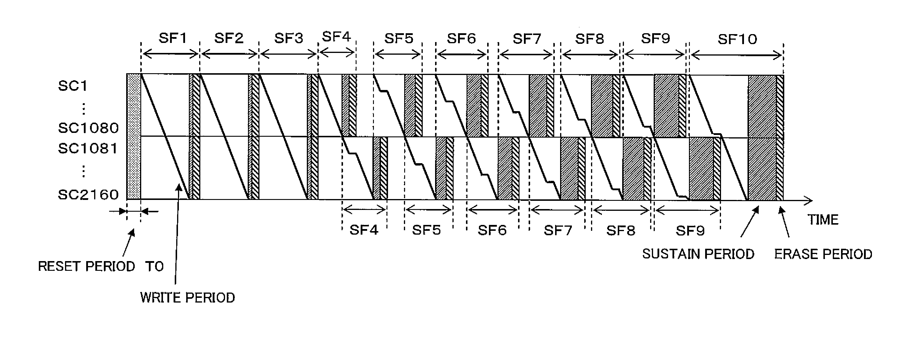
[0199]FIG. 11 is a view showing a sub-field configuration applied to a driving method of the plasma display panel 10 of Embodiment 2. As in the example shown in FIG. 10, vertical axis indicates scan electrodes SC1˜SC2160 and horizontal axis time. The wall voltage adjusting period consists of the erase period. Timings when the write operation is performed are indicated by solid lines, the sustain periods are hatched by oblique lines from right and upper to left and lower, and the erase periods are hatched by oblique lines from left and upper and right and lower. A plasma display apparatus of Embodiment 2 is similar to that of Embodiment 1 shown in FIG. 5 and will not be described repetitively

[0200]The configuration of the sub-fields of Embodiment 2 is different from the sub-field configuration of Embodiment 1 shown in FIG. 10 in that sustain periods which are luminance weights are arranged in decreasing order of length, except for the sub-field SF1. For the sub-field SF2 with a large...

embodiment 3

[0207]FIG. 12 is a view showing a sub-field configuration applied to a driving method of the plasma display panel 10 of Embodiment 3. As in the example shown in FIG. 10, vertical axis indicates scan electrodes SC1˜SC2160 and horizontal axis time. The wall voltage adjusting period consists of the erase period. Timings when the write operation is performed are indicated by solid lines, the sustain periods are hatched by oblique lines from right and upper to left and lower, and the erase periods are hatched by oblique lines from left and upper and right and lower. A plasma display apparatus of Embodiment 3 is similar to that of Embodiment 1 and will not be described repetitively.

[0208]FIG. 12 shows a sub-field configuration in which a sub-field with a highest lighting ratio is a sub-field SF8. The sub-field with a highest lighting ratio in one field includes discharge cells performing sustain discharge, which are largest in number. Therefore, by performing the sustain discharge and the...


PUM


Abstract

In a driving method of a plasma display panel of the present invention, plural display electrode pairs are divided into plural display electrode pair groups and one field is divided into plural sub-fields. The length of the sustain period is compared to the length of the erase period. If the sustain period is longer than the erase period, sustain discharge and erase discharge are performed for each of the display electrode pair groups, while if the sustain period is shorter than the erase period, sustain discharge and erase discharge of one display electrode pair group are synchronized with those of another display electrode pair group. For a sub-field with a largest luminance weight or a sub-field with a highest lighting ratio, sustain discharge and erase discharge of one display electrode pair group are synchronized with those of another display electrode pair group without fail.

Description

TECHNICAL FIELD[0001]The present invention relates to a method of driving a plasma display panel, and a plasma display apparatus using the driving method.BACKGROUND ART[0002]AC surface discharge type panels, which are typical plasma display panels, has a structure in which a number of discharge cells are formed between a front substrate and a back substrate which are placed so as to face each other.[0003]On the front substrate, plural display electrode pairs each including a scan electrode and a sustain electrode are formed so as to extend in parallel with each other. On the back substrate, plural data electrodes are formed so as to extend in parallel with each other. The front substrate and the back substrate are disposed opposite to each other such that the display electrode pairs three-dimensionally cross the data electrodes, and sealed. A discharge gas is filled into an inner discharge space. The discharge cells are formed at portions where the display electrode pairs are opposi...

Claims


Application Information

Patent Timeline
Patent Type & Authority Applications(United States)
IPC IPC(8): G09G3/28G06F3/038G09G3/288G09G3/291G09G3/292G09G3/293G09G3/294G09G3/296G09G3/298
CPCG09G3/2022G09G3/2927G09G3/293G09G2310/0218G09G3/2965G09G2310/0216G09G3/294G09G3/292
Inventor NAKATA, HIDEKIMAKINO, HIROYASUARAI, YASUHIROWAKABAYASHI, TOSHIKAZUKOMINAMI, SATOSHIIZUCHI, MASUMIMATSUSHITA, JUNKO
Owner PANASONIC CORP
Why Eureka
Try Eureka