Plasma display panel

a technology of display panel and plasma, which is applied in the direction of gas discharge electrode, sustain/scan electrode, gas discharge tube, etc., can solve the problems of increased manufacturing cost of pdp, high discharge firing voltage, and uneven discharge, so as to improve the electrode structure and enhance the emission luminance and discharge efficiency

Inactive Publication Date: 2006-05-11
SAMSUNG SDI CO LTD
View PDF6 Cites 0 Cited by
  • Summary
  • Abstract
  • Description
  • Claims
  • Application Information

AI Technical Summary

Benefits of technology

[0014] An embodiment of the present invention provides a plasma display panel that has an improved electrode structure, thereby enhancing emission luminance and discharge efficiency.
[0015] An embodiment of the present invention provides a plasma display panel that uses an electrode made of a metal, thereby improving conductivity.
[0016] An embodiment of the present invention provides a plasma display panel that has an increased aperture ratio.
[0017] An embodiment of the present invention provides a plasma display panel that can structurally compensate for a difference in luminance of discharge cells for respective colors.

Problems solved by technology

Because of this, the discharge is fired partially along the short sides of the discharge cell and thus the discharge may not be diffused smoothly.
However, even when the transparent electrode and the metal electrode are formed together, the transparent electrode is disposed along the periphery of the discharge gap where the discharge occurs, which results in a high discharge firing voltage.
Further, since the material (for example, indium tin oxide or ITO) for the transparent electrode is expensive, the manufacturing cost of the PDP is increased, so that the price competitiveness is lowered.
Further, since the electrode formed in a strip shape on the substrate has a two-layer structure of the transparent electrode and the metal electrode, the manufacturing process is further complicated, which causes the manufacturing cost to be further increased.
Further, when manufacturing the PDP, a substantial difference in thickness according to colors may occur.
Accordingly, the difference in capacitance occurs due to the characteristics of the materials of the phosphor layer and the difference in thickness, which results in a problem in that the emission luminances of the red, green, and blue discharge cells are different from each other.

Method used


Image

  • Plasma display panel
  • Plasma display panel
  • Plasma display panel

Examples


first embodiment

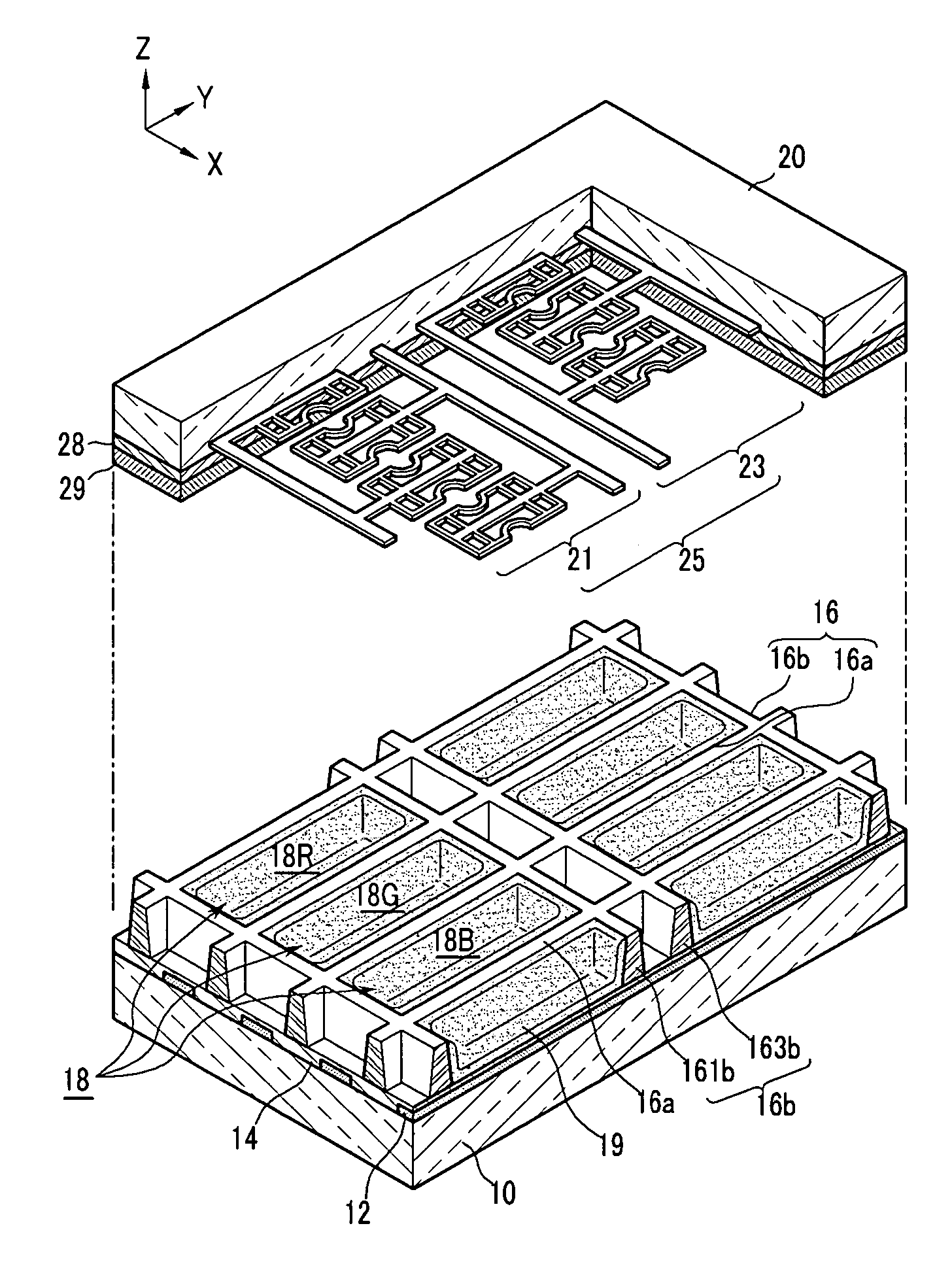
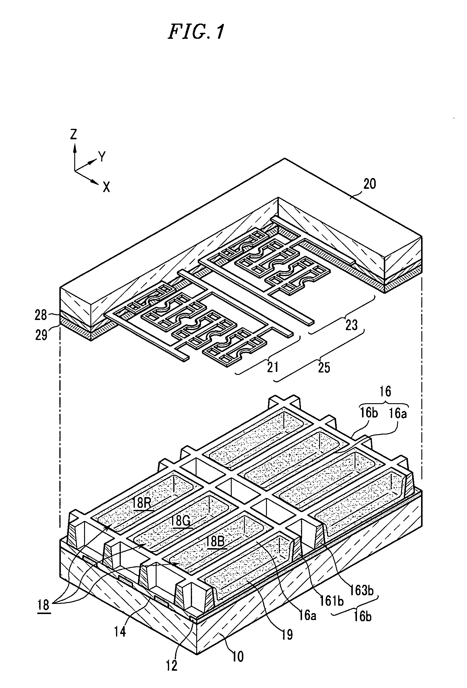
[0041]FIG. 1 is a partially exploded perspective view showing a plasma display panel according to the present invention.

[0042] Referring to FIG. 1, the plasma display panel (hereinafter, referred to as PDP) according to the present embodiment includes a front substrate 20 and a rear substrate 10 that is disposed to face the front substrate 20.

[0043] The front substrate 20 is made of a transparent material, such as glass, through which a visible light beam transmits to display an image.

[0044] Display electrodes 25 are formed on the lower surface of the front substrate 20. In the present embodiment, the display electrodes 25 are geometrically formed in linear shapes in order to increase an aperture ratio of a discharge cell. The display electrodes 25 will be described below in more detail.

[0045] The display electrodes 25 may be covered and filled with a dielectric layer (or a first dielectric layer) 28 made of a dielectric material, such as PbO, B2O3, SiO2, or the like. The dielect...

second embodiment

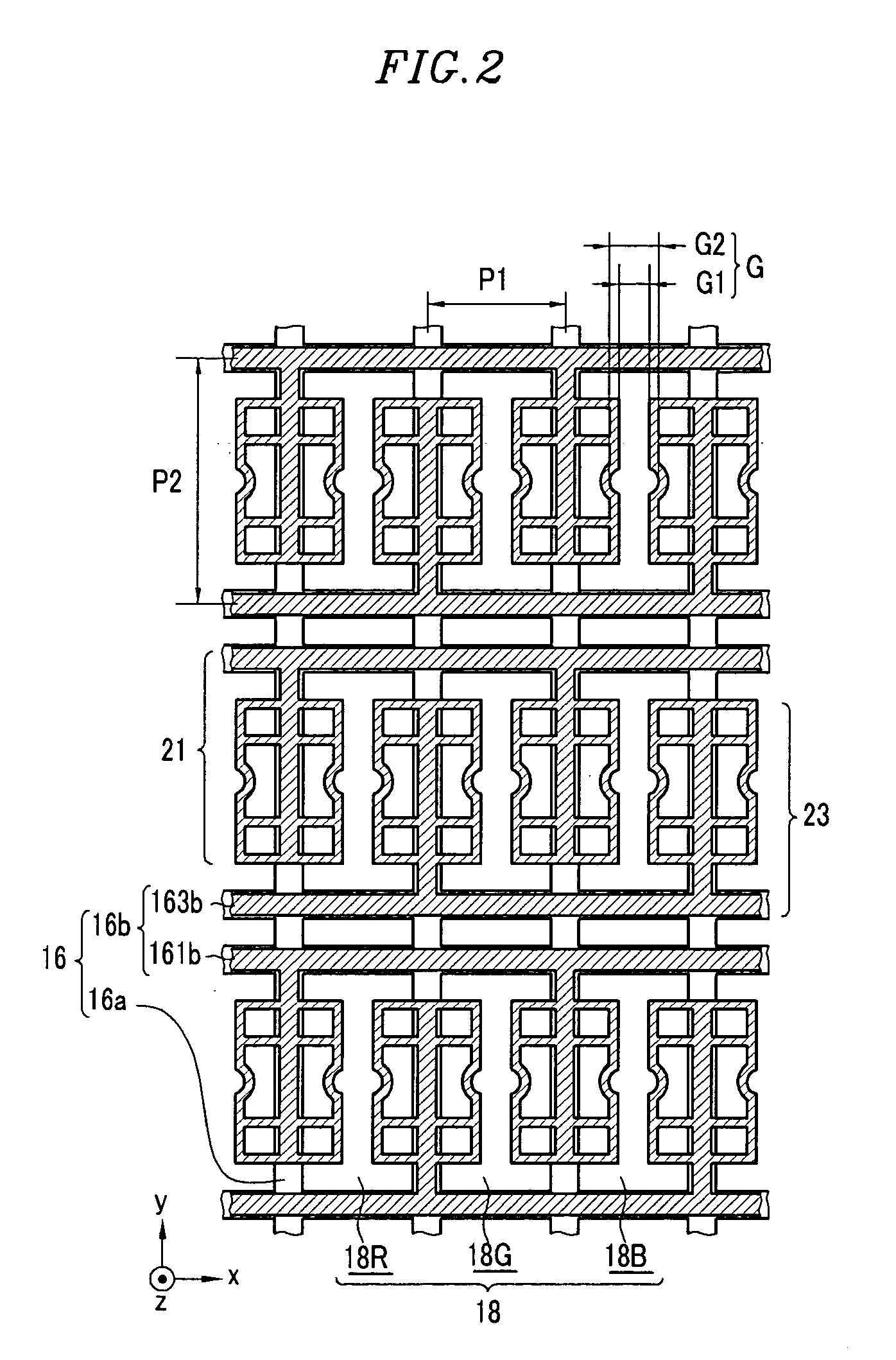
[0085]FIG. 7 is a plan view illustrating the positional relationship between display electrodes and barrier ribs according to the present invention.

[0086] A scan electrode 41 (having a linear portion 41a and a protruded portion 41b) and a sustain electrode 43 (having a linear portion 43a and a protruded portion 43b) of the second embodiment also have substantially the same configurations as described above, except that second concave portions C2 are formed in second electrode portions 413b and 433b, respectively.

[0087] The second concave portions C2 are in one embodiment connected to ends of first portions 411 and 431, respectively. Further, the second electrode portions 413b and 433b of second portions 413 and 433 may obliquely connect first electrode potions 413a and 433a of the second portions 413 and 433 to the first portions 411 and 431, respectively.

third embodiment

[0088]FIG. 8 is a plan view illustrating the positional relationship between display electrodes and barrier ribs according to the present invention.

[0089] The discharge cells 18 are divided into the red discharge cells 18R, the green discharge cells 18G, and the blue discharge cells 18B according to the colors represented by the phosphor layer coated on the respective discharge cells 18.

[0090] Also, as similar to the first and second embodiments described above, a scan electrode 61 and a sustain electrode 63 have linear portions 61a and 63a and protruded portions 61b and 63b, respectively. The protruded portions 61b and 63b are disposed in a pair of adjacent discharge cells on the respective vertical barrier ribs 16a.

[0091] In the third embodiment, in order to reduce the difference in luminance by colors of the discharge cells, the protruded portions 61b and 63b formed corresponding to the discharge cell for one color are formed to be larger than the protruded portions 63a and 63b...


PUM


Abstract

A plasma display panel has an improved display electrode, thereby enhancing emission luminance. The plasma display panel includes a front substrate and a rear substrate that face each other and between which a space is formed, barrier ribs that define a plurality of discharge cells in the space between the front substrate and the rear substrate, address electrodes that extend in a first direction to intersect the discharge cells, phosphor layers that are respectively formed within the discharge cells, and first electrodes and second electrodes having linear portions that are formed in a second direction to intersect the first direction and protruded portions that extend in the first direction from the linear portions and face each other in the second direction within the discharge cells so as to form discharge gaps, respectively.

Description

CROSS-REFERENCE TO RELATED APPLICATION [0001] This application claims priority to and the benefit of Korean Patent Application No. 10-2004-0090843, filed in the Korean Intellectual Property Office on Nov. 9, 2004, the entire content of which is incorporated herein by reference. BACKGROUND OF THE INVENTION [0002] 1. Field of the Invention [0003] The present invention relates to a plasma display panel, and more particularly, a plasma display panel that has an improved structure of a display electrode to thereby enhance emission luminance. [0004] 2. Description of the Related Art [0005] Generally, a plasma display panel (hereinafter, referred to as PDP) is a display device in which vacuum ultraviolet rays emitted from plasma through gas discharge excite phosphors to generate visible light, thereby realizing images. In a PDP, a large screen of 60 inches or more can be implemented to have a thickness of no more than 10 cm. Further, the PDP is a self-emitting device, like a cathode ray tu...

Claims


Application Information

Patent Timeline
Patent Type & Authority Applications(United States)
IPC IPC(8): H01J17/49
CPCH01J11/12H01J11/24H01J11/32H01J2211/245H01J2211/323H01J2211/326H01J2211/225
Inventor EOM, KI-JONG
Owner SAMSUNG SDI CO LTD
Why Eureka
Try Eureka