Dual Interconnection in Stacked Memory and Controller Module

a controller module and dual structure technology, applied in the direction of semiconductor devices, semiconductor/solid-state device details, electrical apparatus, etc., can solve the problems of limiting the overall speed of operation of a multi-chip circuit, the transmission delay of the extended signal path between horizontally mounted chips becomes a significant factor in limiting the speed of operation of the multi-chip circuit, and the speed of the conventional construction of multi-chip circuits. achieve the effect of improving the inspection and access of contacts, and improving the capacity

Inactive Publication Date: 2011-07-14
WAFER LEVEL PACKAGING PORTFOLIO
View PDF5 Cites 29 Cited by
  • Summary
  • Abstract
  • Description
  • Claims
  • Application Information

AI Technical Summary

Benefits of technology

[0015]In yet another embodiment, the invention provides a dual structure of interconnections in a stack of chips that uses less space in the circuit area of the chips, and thereby provides lower cost and better high-speed performance than offered by exclusive use of either ECs or TSVs alone.
[0018]This invention further provides improved ECs and methods of fabricating the ECs. In a first embodiment, an EC that is at least partly recessed (embedded) into the sidewall of a chip is provided, such that a plurality of embedded ECs along the edge of a chip can have uniform pad pitch but different cross-sectional areas according to the depth of embedding, thereby providing economy through tailoring of the ECs according to current carrying requirements. In a second embodiment, an EC having a gull lead that protrudes outside the chip perimeter and below the rear surface of the chip is provided, thereby providing improved inspection and access to contacts.

Problems solved by technology

Conventional construction of multichip circuits has speed, cost, and reliability limitations.
Interconnecting traces (also known as wires) along a printed circuit board between two IC chips, and / or along the surface of an IC chip, including wire bonds from a chip to the board, introduce signal transmission delay related to the length of the signal path.
As computer operating and memory access speeds increase, such as with the DDR3, DDR4, GDDR4, and XDR interface technologies known in the art, transmission delay in the extended signal paths between horizontally mounted chips becomes a significant factor in limiting the overall speed of operation of a multichip circuit.
The longer a circuit trace or signal path, the greater the capacitive load, increasing the time required to charge or discharge the signal path in digital signal transmission.
Similarly, at high operating frequency the series inductance of the signal path can affect signal rise time, thereby again, limiting the clock speed of a digital signal.
This conventional memory card architecture not only fosters signal degradation, but component degradation as well.
Because of a disparity in thermal expansion between silicon chips and the circuit boards on which silicon chips are typically mounted, thermal cycling failure plays an important role in reducing the operating life of a multichip module having horizontally mounted chips (i.e., wherein one of the chip's large surface areas is mounted against the circuit board).
Wire bonding used in conventional multichip circuits also has a cost issue.
Gold wires now account for a significant portion of packaging cost.
However, serpentine signal paths that include EWCs coupled with circuit traces on the surface of a chip do not provide the shortest circuit path, and delay between some critical circuit portions in a stacked multichip circuit.
TSVs, however, take up valuable “real estate” within the active circuit area of a chip.
TSVs have a further recently discovered disadvantage that crystal structure defects can develop within a chip in the circuit area near closely spaced TSVs, which can reduce reliability.

Method used


Image

  • Dual Interconnection in Stacked Memory and Controller Module
  • Dual Interconnection in Stacked Memory and Controller Module
  • Dual Interconnection in Stacked Memory and Controller Module

Examples


embodiment 300

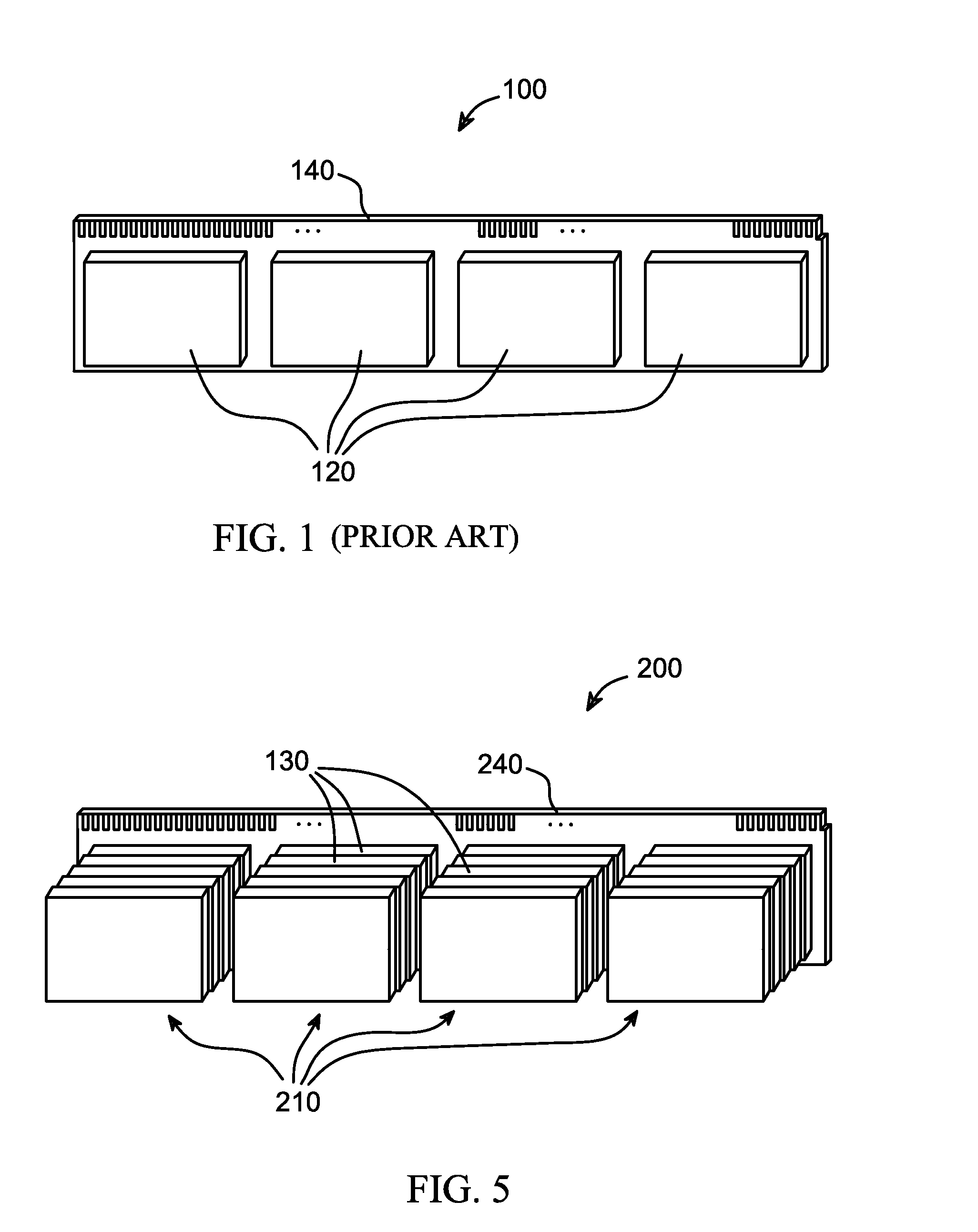
[0072]FIG. 6 depicts an embodiment 300 having four chips 130 stacked on a pin-grid type circuit board 340. The memory of each chip 130 is equivalent to the memory of the respective chips 120 of FIG. 1. However, through incorporating the design embodiments and features described herein, the chips 130 can be stacked, thereby achieving a more compact connection configuration that can have substantially the same capacity as the prior art memory module of FIG. 1. The pin grid configuration 300 of FIG. 6 is presented only as one alternate embodiment by which a more compact chip stack can be coupled to a motherboard or other electronic assembly component.

Compact Memory and Controller Modules Through Stacking with Dual Interconnection:

embodiment 400

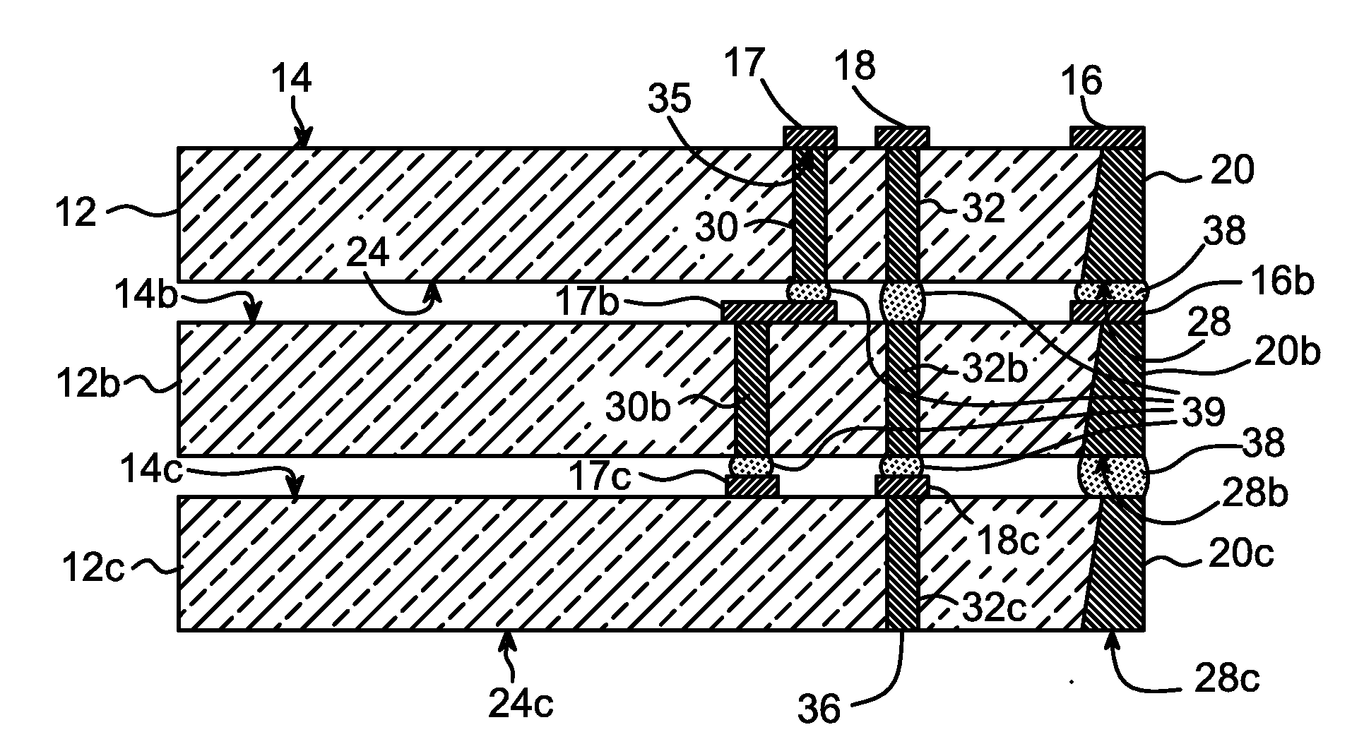
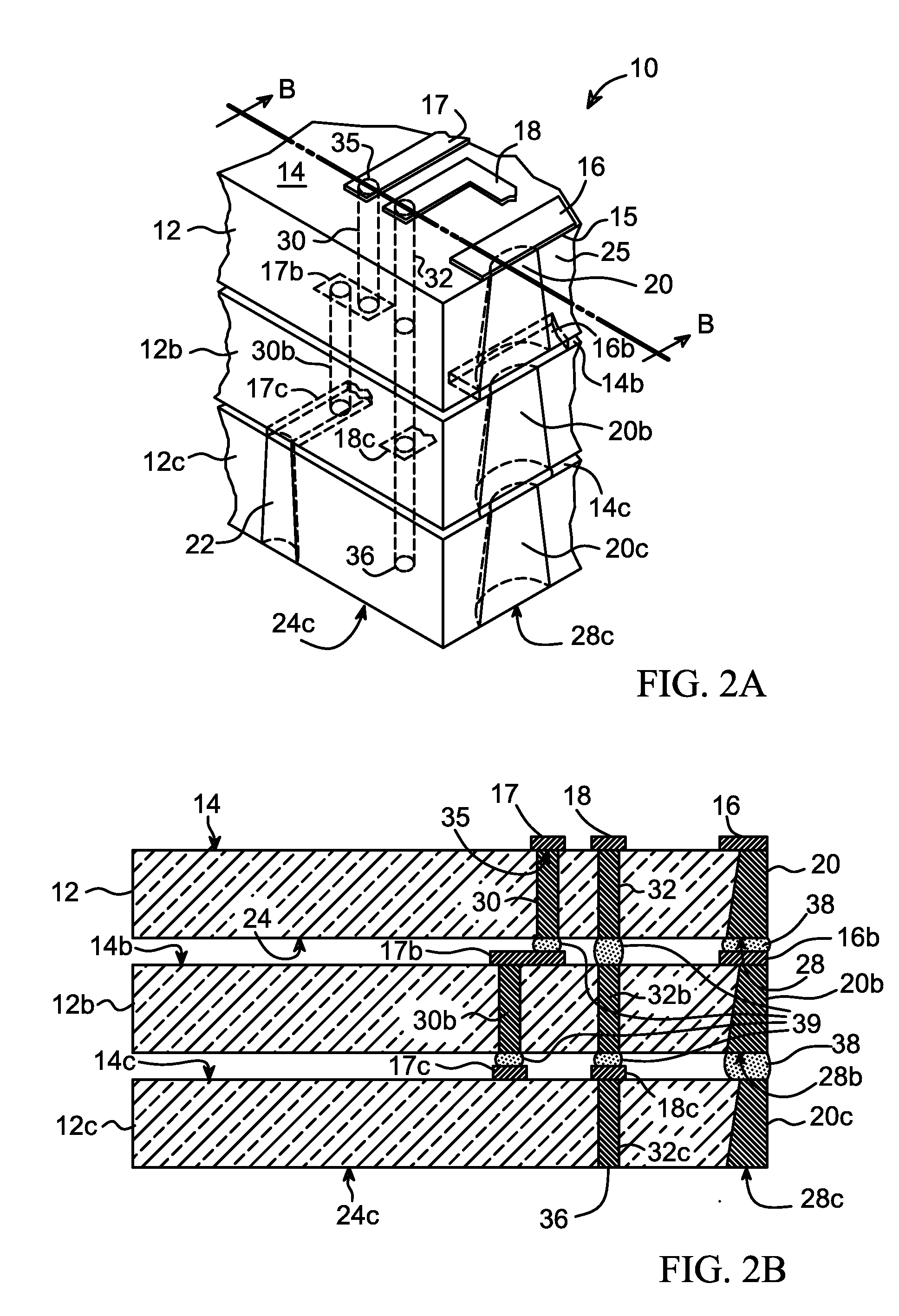
[0073]Another application can be appreciated by the embodiment 400 depicted in FIG. 7. The memory chips 130 of FIG. 7 are fabricated with both ECs and TSVs, as described herein, and configured to segregate signals through these respective transmission paths, as further described herein. The chips 130 are electrically interconnected in a stack configuration 210 utilizing interconnection features taught in conjunction with FIGS. 2A-4B. The stacked memory chips 130 are mounted on top of a memory controller chip 420.

[0074]Significant advantages ensue from the design of the memory module 400 in FIG. 7, in comparison to the prior art designs. Electrical transmission of a digital signal may require the charging or discharging of a conductive path to certain requisite voltage levels. As a consequence, the clock speed of a memory controller is limited, at least in part, by the time it takes to charge or discharge a conductive path between the controller and a memory chip controlled by the me...

embodiment 450

[0075]FIG. 8 depicts an embodiment 450 similar to FIG. 7, but wherein stacked memory chips 130 are disposed on opposite sides of the memory controller 420, further reducing the maximum transmission distance between the controller and the most distal memory chips coupled to the memory module.

Method of Fabricating a Stacked Chip Module Incorporating Dual Interconnection:

[0076]FIG. 9 depicts a sequence of steps 500 that illustrate, by way of example, a design and fabrication process for manufacturing a semiconductor module comprising a stack of IC chips interconnected by ECs and TSVs, according to features described above. Throughout FIGS. 5-10, the terms “semiconductor module” and “IC stack” are used somewhat interchangeably, with specific application toward semiconductor modules such as FIGS. 6 and 7, in which a single stack of IC chips is coupled with a substrate, memory controller, or other electronic structure (e.g., elements 340, 420 in FIGS. 6, 7, 8). This specific scope of the ...


PUM


Abstract

A chip package transmitting slow speed signals via edge connectors and high speed signals by means of through-silicon-vias. The edge connectors are formed in recesses formed in the sidewalls of the package.

Description

[0001]This application incorporates by reference U.S. Pat. No. 5,910,687 to Chen, et al., U.S. Pat. No. 5,505,816 to Barnes, et al., U.S. Pat. No. 5,656,547 to Richards, et al., U.S. Pat. No. 6,911,392 to Bieck, et al., and “3-D Through-Silicon Vias Become a Reality”, by Jan Vardaman, Semiconductor International, No. 6, Jun. 1, 2007.BACKGROUND OF THE INVENTION[0002]1. Field of the Invention[0003]The present invention relates generally to the field of semiconductor device manufacturing, and more particularly to an improved dual structure and method of interconnection for a multichip electronic circuit, such as a memory module.[0004]2. Description of the Background Art[0005]A semiconductor integrated circuit (IC) chip, also called a die, is typically formed in a polygonal shape comprising an active surface, also known as the front side or top side of the chip, a rear surface or rear side parallel to the active surface, but facing in the opposite direction, and edges extending between ...

Claims


Application Information

Patent Timeline
Patent Type & Authority Applications(United States)
IPC IPC(8): H01L23/48
CPCH01L23/481H01L24/16H01L2924/10253H01L24/40H01L24/41H01L24/73H01L25/0657H01L2224/13009H01L2225/06513H01L2225/06527H01L2225/06541H01L2225/06551H01L2924/01013H01L2924/01078H01L2924/01079H01L2924/01082H01L2924/14H01L2924/19041H01L2924/19043H01L2924/30105H01L2924/30107H01L2924/3011H01L2924/01005H01L2924/01006H01L2924/01019H01L2924/01023H01L2924/01033H01L2924/01055H01L2924/01075H01L2924/014H01L2924/00H01L2224/05009H01L2224/05548H01L2224/0557H01L2224/05001H01L2924/00014H01L24/06H01L2224/06181H01L24/05H01L2224/02372H01L2224/0401H01L2224/05599H01L2224/05099H01L2224/37099
Inventor MARCOUX, PHIL P.
Owner WAFER LEVEL PACKAGING PORTFOLIO
Why Eureka
Try Eureka