Method of manufacturing multi-layer coil and multi-layer coil device

a multi-layer coil and coil device technology, applied in the direction of magnets, inductances, magnetic bodies, etc., can solve the problems of ineffective reduction of direct current resistance, inability to effectively raise saturation current, and limited size and thickness of chokes, so as to achieve effective enhancement of multi-layer coil characteristics, less space, and increase the area of the cross section of the pillar

Active Publication Date: 2015-02-05
CYNTEC
View PDF6 Cites 103 Cited by
  • Summary
  • Abstract
  • Description
  • Claims
  • Application Information

AI Technical Summary

Benefits of technology

[0010]As mentioned in the above, the invention forms the multi-layer coil on the substrate by a plating process with varied current densities, so as to replace the conventional winding-type coil with the plated multi-layer coil. The plated multi-layer coil occupies less space than the conventional winding-type coil such that the multi-layer coil device can be miniaturized easily and the characteristics of the multi-layer coil device can be enhanced effectively (e.g. increasing the area of the cross section of the pillar, reducing the direct current resistance, increasing the saturation current, and so on).

Problems solved by technology

However, since the winding space S has to be reserved for winding the wire 12, the area of the cross section of the pillar 100 is limited accordingly, so that saturation current cannot be raised effectively and direct current resistance cannot be reduced effectively.
Furthermore, compared with the conventional winding-type coil structure, the wire has to be wound around the pillar by mechanical operation such that the size and thickness of the choke are limited accordingly (e.g. the size of the wire is reduced, the yield rate is reduced due to incorrect operation, and so on).

Method used


Image

  • Method of manufacturing multi-layer coil and multi-layer coil device
  • Method of manufacturing multi-layer coil and multi-layer coil device
  • Method of manufacturing multi-layer coil and multi-layer coil device

Examples


Embodiment Construction

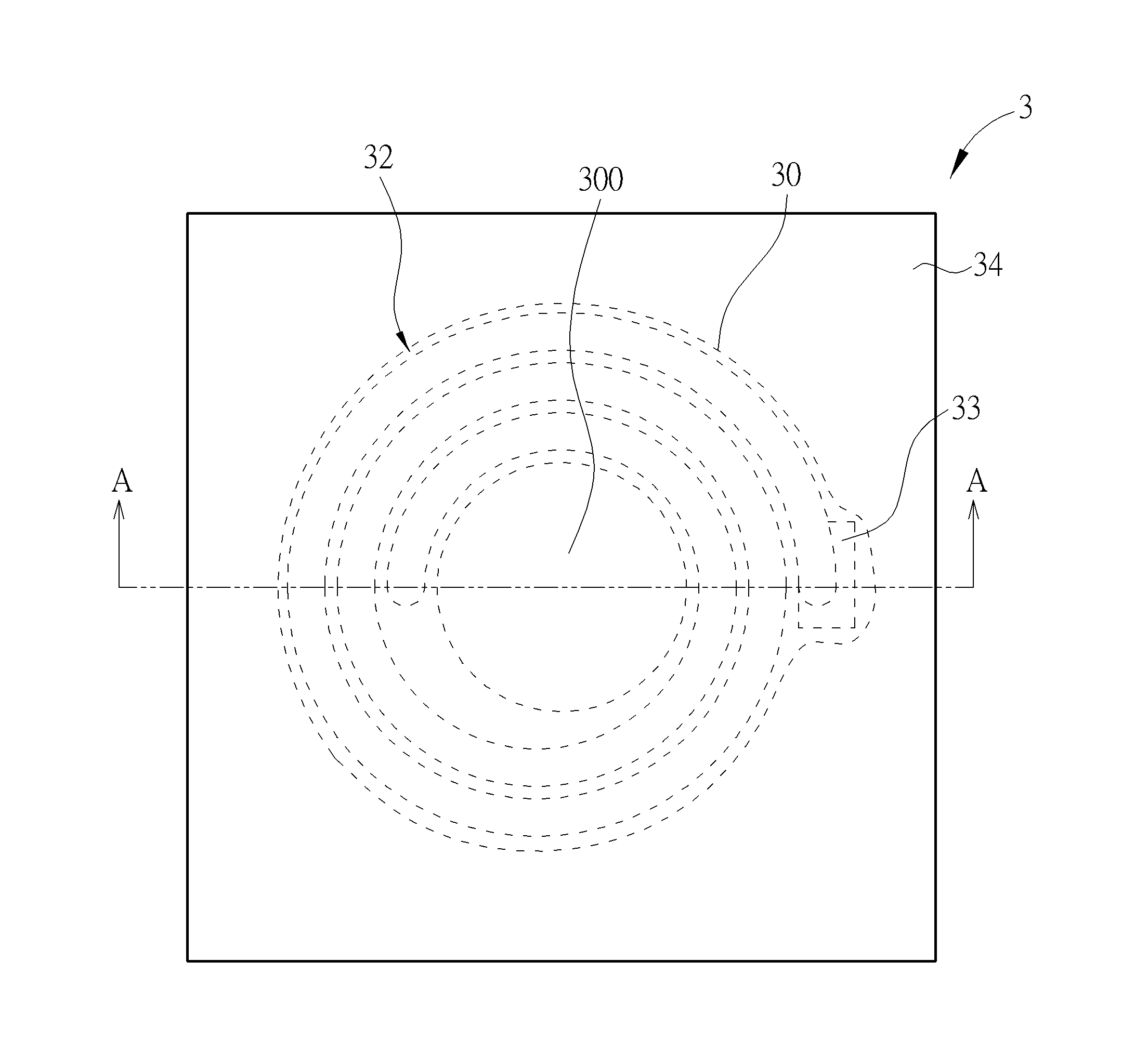
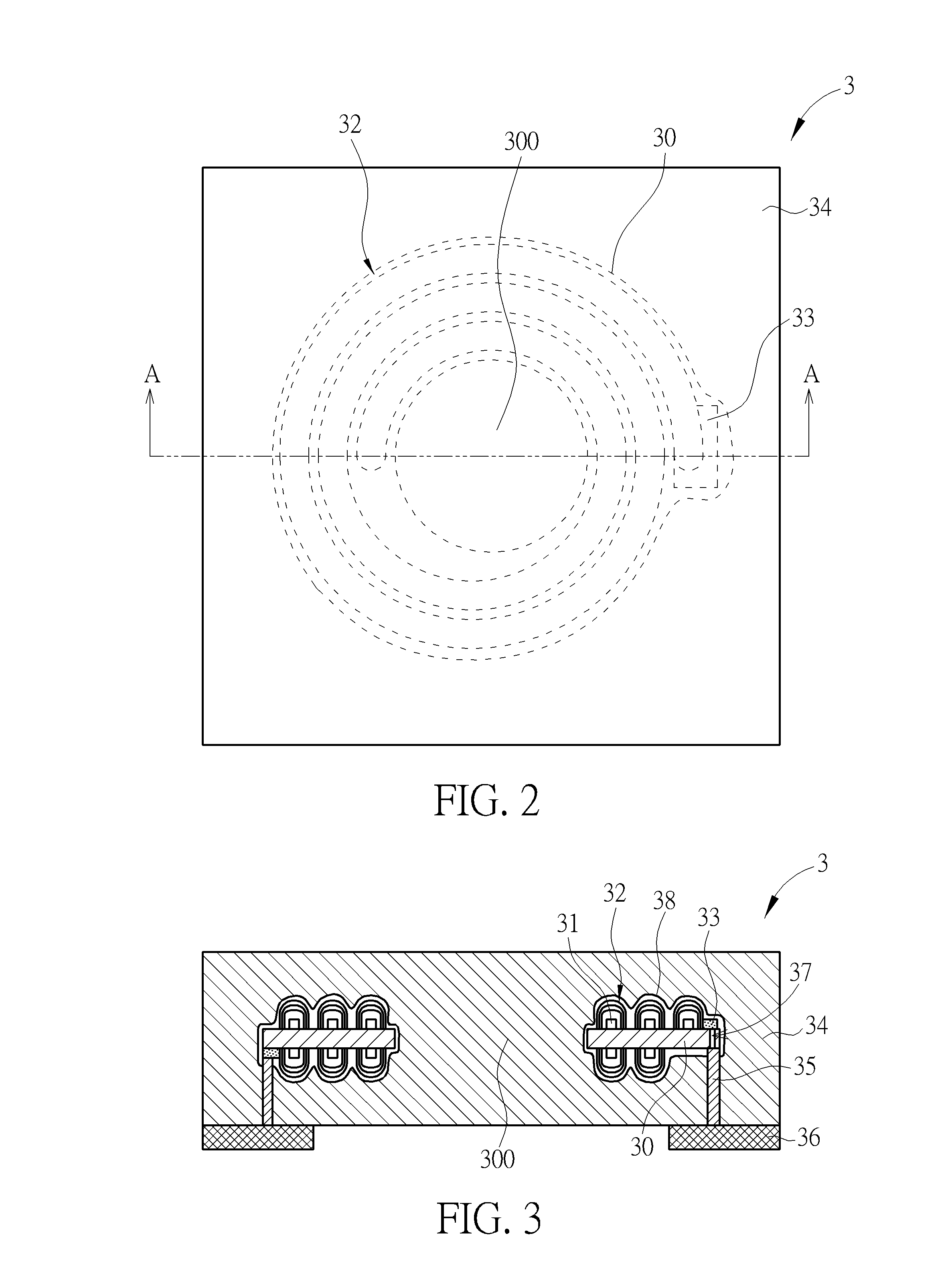
[0018]Referring to FIGS. 2 to 5, FIG. 2 is a top view illustrating a multi-layer coil device 3 according to an embodiment of the invention, FIG. 3 is a cross-sectional view illustrating the multi-layer coil device 3 along line A-A shown in FIG. 2, FIG. 4 is an enlarged view illustrating parts of the multi-layer coil 32 shown in FIG. 3, and FIG. 5 is a flowchart illustrating a method of manufacturing the multi-layer coil device 3 shown in FIG. 2 and the multi-layer coil 32 shown in FIG. 3. The multi-layer coil device 3 of the invention may be a current power module or component, a radio frequency component, a chip inductor, a choke, a transformer, or other magnetic components. According to this embodiment, the multi-layer coil device 3, such as a magnetic component, comprises a substrate 30, a multi-layer coil 32, a magnetic body 34 and a pair of electrodes 36. The multi-layer coil 32 is formed on the substrate 30 by a plating process with varied current densities. The magnetic body ...


PUM

PropertyMeasurementUnit
heightaaaaaaaaaa
aspect ratioaaaaaaaaaa
width WOaaaaaaaaaa

Abstract

A method of manufacturing a multi-layer coil includes steps of providing a substrate; forming a seed layer on the substrate; and plating the seed layer with N coil layers by N current densities according to N threshold ranges, so as to form the multi-layer coil on the substrate, wherein an i-th current density of the N current densities is lower than an (i+1)-th current density of the N current densities. A first coil layer of the N coil layers is plated on the seed layer by a first current density of the N current densities. When an aspect ratio of an i-th coil layer of the N coil layers is within an i-th threshold range of the N threshold ranges, an (i+1)-th coil layer of the N coil layers is plated on the i-th coil layer by the (i+1)-th current density.

Description

BACKGROUND OF THE INVENTION[0001]1. Field of the Invention[0002]The invention relates to a method of manufacturing a multi-layer coil and a multi-layer coil device and, more particularly, to a method of manufacturing a multi-layer coil by a plating process with varied current densities and a multi-layer coil device utilizing the multi-layer coil.[0003]2. Description of the Prior Art[0004]A choke, which is one kind of multi-layer coil device, is used for stabilizing a circuit current to achieve a noise filtering effect, and a function thereof is similar to that of a capacitor, by which stabilization of the current is adjusted by storing and releasing electrical energy of the circuit. Compared to the capacitor that stores the electrical energy by an electrical field (electric charge), the choke stores the same by a magnetic field.[0005]In the past, the chokes are generally applied in electronic devices such as DC / DC converters and battery chargers, and applied in transmission devices ...

Claims


Application Information

Patent Timeline
Patent Type & Authority Applications(United States)
IPC IPC(8): H01F41/04H01F27/28H01F5/00
CPCH01F41/042H01F2027/2809H01F27/2804H01F5/003C25D5/02H01F17/0006H01F27/292H01F2017/0066Y10T29/4902
Inventor WANG, CHUNG-HSIUNGCHIANG, LANG-YICHANG, WEI-CHIENLIN, YU-HSIN
Owner CYNTEC
Why Eureka
Try Eureka