
Single layer touch panel with segmented drive and sense electrodes

a single layer, drive electrode technology, applied in the direction of instruments, computing, electric digital data processing, etc., can solve the problems of high manufacturing cost of touch sensor panels, thin devices, and single substrate row and column lines, so as to reduce the number of drive electrodes in each column and reduce the use of connecting traces

Active Publication Date: 2012-11-27
APPLE INC
View PDF73 Cites 96 Cited by
  • Summary
  • Abstract
  • Description
  • Claims
  • Application Information

AI Technical Summary

Benefits of technology

This approach allows for larger touch sensor panels with reduced resistance in connecting traces, maintaining sensitivity and uniformity while reducing manufacturing costs by eliminating the need for border metal on glass routing.

Problems solved by technology

Such touch sensor panels can be expensive to manufacture, because processing must be performed on two different substrates.
In addition, the use of two substrates can result in a thicker device.
However, touch sensor panels having row and column lines formed on the bottom and top sides of a single substrate can also be expensive to manufacture, because thin-film processing steps must be performed on both sides of the glass substrate, which requires protective measures for the processed side while the other side is being processed.
As a result, more connecting traces have to be squeezed into the limited amount of space between the columns of drive line bricks to connect each row.
This may require the connecting traces to be made narrower, which result in an increase in the resistance of the traces.
As a result, the stimulating signal bandwidth may be reduced due to the increased time constant introduced by these narrower, higher resistance drive lines, causing the touch panel to be less sensitive and more non-uniform.

Method used


Image

  • Single layer touch panel with segmented drive and sense electrodes
  • Single layer touch panel with segmented drive and sense electrodes
  • Single layer touch panel with segmented drive and sense electrodes

Examples


Embodiment Construction

[0023]In the following description of preferred embodiments, reference is made to the accompanying drawings which form a part hereof, and in which it is shown by way of illustration specific embodiments in which the invention can be practiced. It is to be understood that other embodiments can be used and structural changes can be made without departing from the scope of the embodiments of this invention.

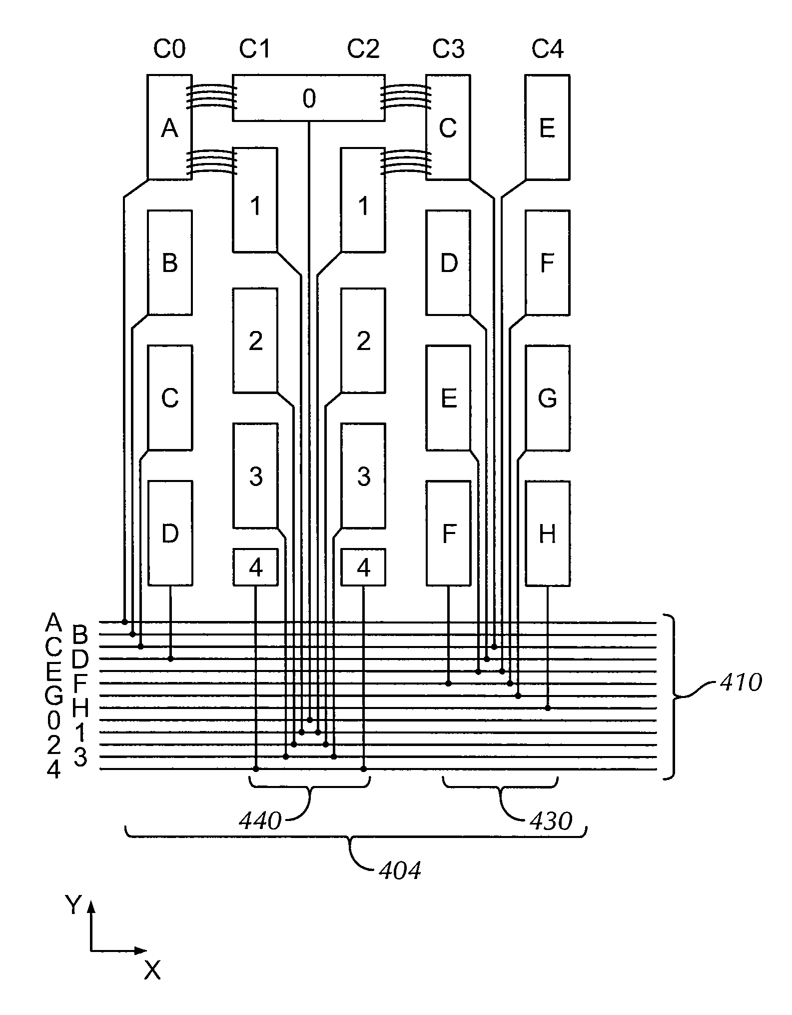
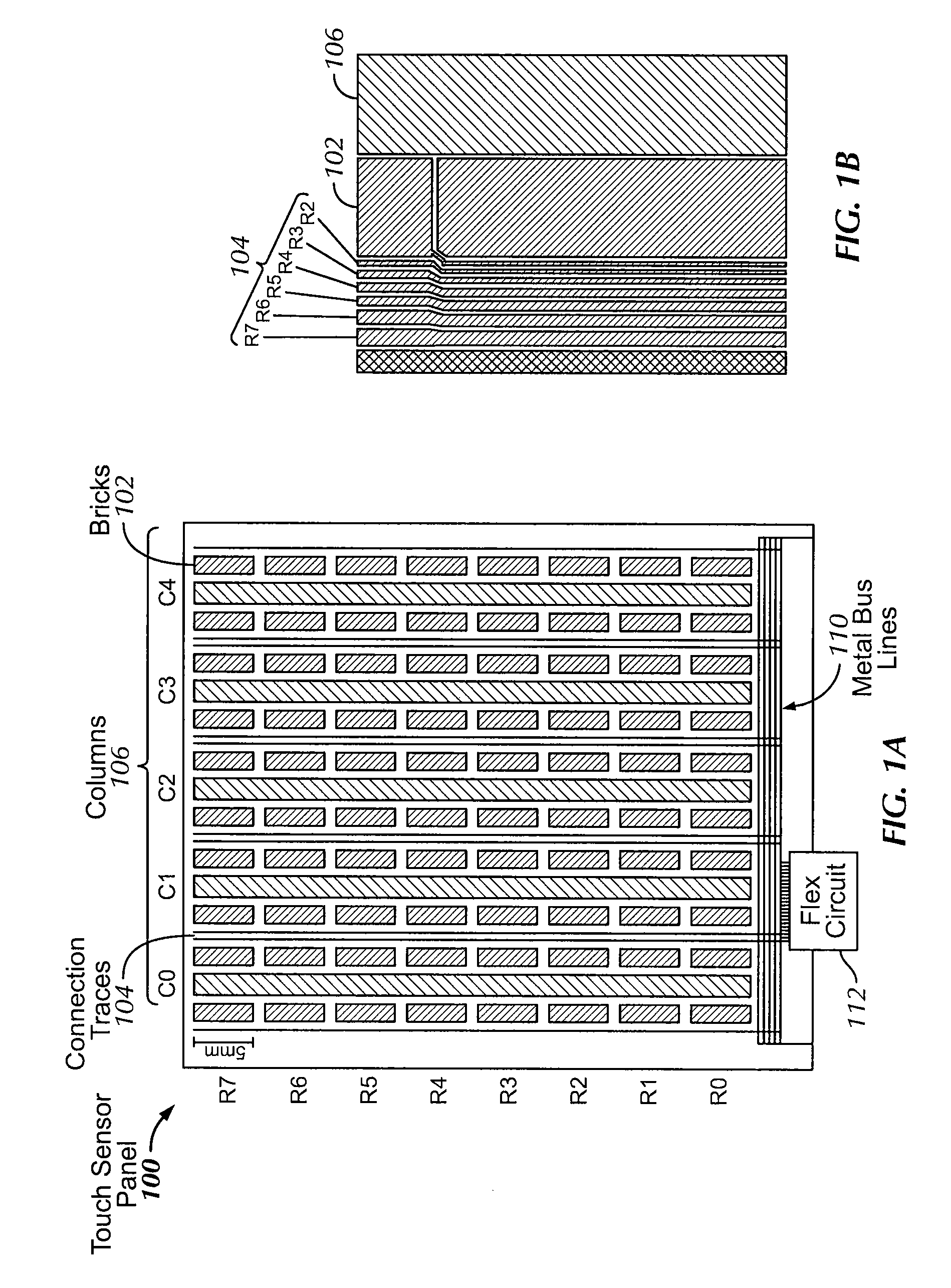
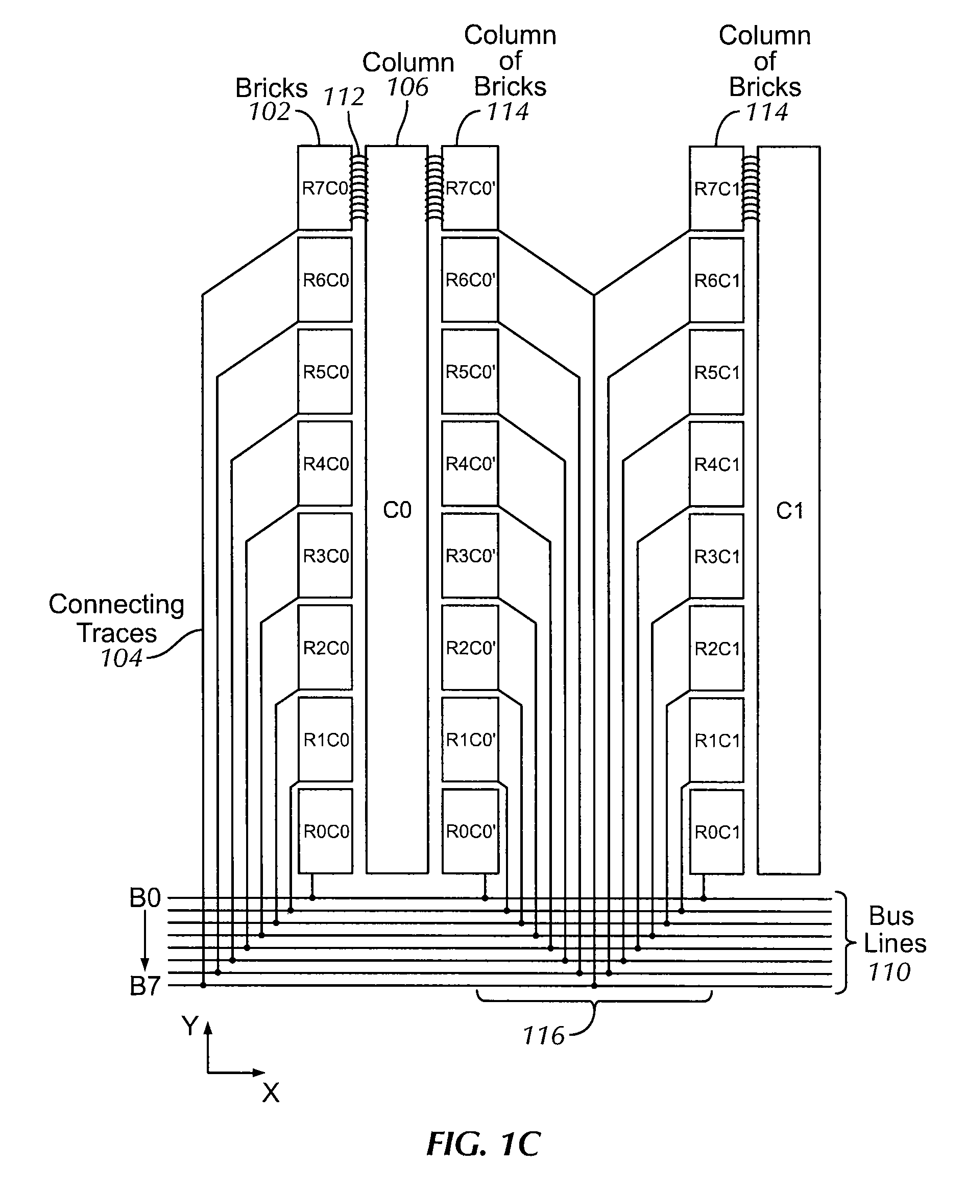
[0024]In general, this relates to a single-layer touch sensor panel in which both the drive and sense lines include segmented electrodes. By segmenting both drive and sense lines and staggering the segmented electrodes in various patterns, embodiments of the invention can reduce the number of drive (or sense) electrodes in each column and reduce the number of connecting traces required to connect the drive (or sense) electrodes. As a result, a larger touch sensor panel can be fabricated while maintaining a more uniform signal strength in the drive lines. An additional benefit of havi...


PUM


Abstract

A touch sensor panels having segmented electrodes for both the drive and sense lines. The touch sensor panel may include a number of columns of sense electrodes and a number of rows of drive electrodes. Each of the drive and sense electrodes are connected to one of the metal bus lines using a connecting trace. Pixels on the touch sensor panel are formed by the unique pairings of individual drive electrodes and their adjacent sense electrodes. Electrically, the mutual capacitance of one touch-sensing pixel can be distinguished from the mutual capacitance of another touch sensing pixel because the two mutual capacitances are formed with combinations of different drive electrodes and sense electrodes. In one embodiment, the drive electrodes and sense electrodes in adjacent columns are staggered horizontally with respect to each other by half a Y-pitch of the electrodes.

Description

FIELD OF THE INVENTION[0001]This relates generally to input devices for computing systems, and more particularly, to a touch sensor panel capable of being fabricated on a single side of a substrate.BACKGROUND OF THE INVENTION[0002]Many types of input devices are presently available for performing operations in a computing system, such as buttons or keys, mice, trackballs, touch sensor panels, joysticks, touch screens and the like. Touch screens, in particular, are becoming increasingly popular because of their ease and versatility of operation as well as their declining price. Touch screens can include a touch sensor panel, which can be a clear panel with a touch-sensitive surface. The touch sensor panel can be positioned in front of a display screen so that the touch-sensitive surface covers the viewable area of the display screen. Touch screens can allow a user to make selections and move a cursor by simply touching the display screen via a finger or stylus. In general, the touch ...

Claims


Application Information

Patent Timeline
Patent Type & Authority Patents(United States)
IPC IPC(8): G06F3/045G06F3/041
CPCG06F3/044G06F3/0443G06F3/04164G06F3/04166
Inventor HOTELLING, STEVE PORTERGRUNTHANER, MARTIN PAULYOUSEFPOR, MARDUKE
Owner APPLE INC
Learn More