Method for Making a Planar Concentrating Solar Cell Assembly with Silicon Quantum Dots
a solar cell and quantum dots technology, applied in the field of concentrating solar cell assemblies, can solve the problems of complex and expensive solar cell assemblies, difficult to fit solar cell assemblies in buildings, and inconvenient maintenance of solar cells
- Summary
- Abstract
- Description
- Claims
- Application Information
AI Technical Summary
Benefits of technology
Problems solved by technology
Method used
Image
Examples
first embodiment
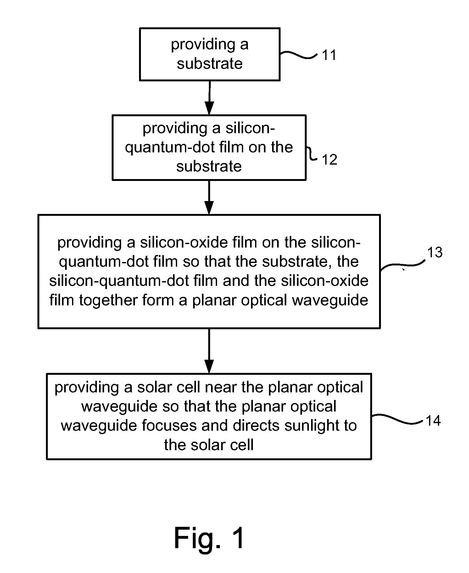
Referring to FIG. 1, a method for making a silicon-quantum-dot planar concentrating solar cell assembly according to the present invention is shown.
Referring to FIGS. 1 and 2, at 11, there is provided a substrate 20. The substrate 20 is a transparent plate made of glass, plastics or resin. The refractive index of the substrate 20 is larger than that of the air so that total reflection could occur at the interface between the substrate 20 and the air.
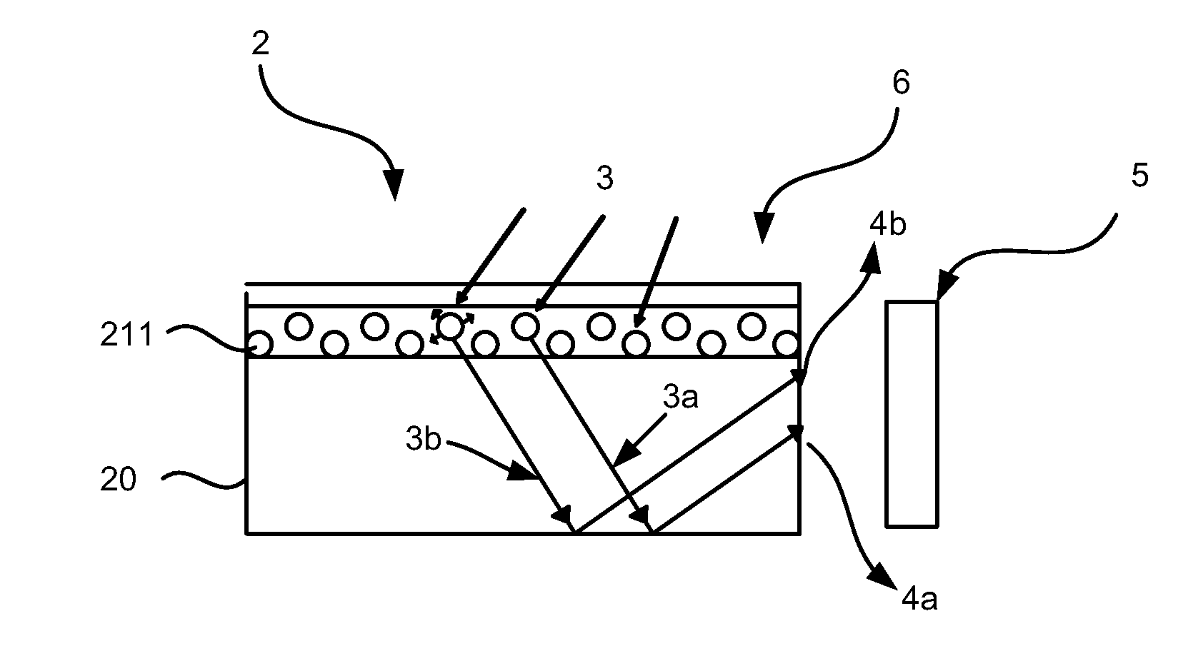
Referring to FIGS. 1 and 3, at 12, a silicon-quantum-dot film is provided on the substrate 20 based on a physical or chemical method. The thickness of the silicon-quantum-dot film 21 is 0.1 to 100 micrometers. The silicon-quantum-dot film 21 includes silicon quantum dots 211 evenly distributed in silicon nitride or silicon oxide. The size of the silicon quantum dots 211 is 1 to 10 nanometers.
Referring to FIGS. 1 and 4, at 13, a silicon-oxide film 22 is provided on the silicon-quantum-dot film 21. Thus, the substrate 20, the silicon-quant...
second embodiment
Referring to FIG. 6, a method for making a silicon-quantum-dot planar concentrating solar cell assembly according to the present invention is shown.
Referring to FIGS. 6 and 7, at 11a, there is provided a substrate 20. The substrate 20 is a transparent plate made of glass, plastics or resin.
At 12a, a silicon-quantum-dot film 21 is provided on the substrate 20 according to a physical or chemical method. The thickness of the silicon-quantum-dot film 21 is 0.1 to 100 micrometers. The silicon-quantum-dot film 21 includes silicon quantum dots 211 evenly distributed in silicon nitride or silicon oxide. The size of the silicon quantum dots 211 is 1 to 10 nanometers.
At 13a, the two foregoing steps are repeated for a predetermined number of times to provide the predetermined number of optical units each including a substrate 20 and a silicon-quantum-dot film 21. The optical units are piled. Then, a silicon-oxide film 22 is provided on the silicon-quantum-dot film 21 of one of the optical unit...
PUM
 Abstract
Description
Claims
Application Information


