HIGH VOLTAGE SCRMOS IN BiCMOS PROCESS TECHNOLOGIES

a technology of bicmos and process technology, applied in the field of integrated circuits, can solve the problems of device damage, degraded reliability of metal oxide semiconductor (mos) transistors integrated with silicon controlled rectifier devices,

Active Publication Date: 2011-07-28
TEXAS INSTR INC
View PDF3 Cites 12 Cited by
  • Summary
  • Abstract
  • Description
  • Claims
  • Application Information

AI Technical Summary

Benefits of technology

[0004]The following presents a simplified summary in order to provide a basic understanding of one or more aspects of the invention. This summary is not an extensive overview of the invention, and is neither intended to identify key or critical elements of the invention, nor to delineate the scope thereof. Rather, the primary purpose of the summary is to present some concepts of the invention in a simplified form as a prelude to a more detailed description that is presented later.

Problems solved by technology

Metal oxide semiconductor (MOS) transistors integrated with silicon controlled rectifier (SCR) devices may exhibit degraded reliability from high voltage transients such as ESD events.
Localized charge carrier injection by this mechanism may cause device damage.

Method used


Image

  • HIGH VOLTAGE SCRMOS IN BiCMOS PROCESS TECHNOLOGIES
  • HIGH VOLTAGE SCRMOS IN BiCMOS PROCESS TECHNOLOGIES
  • HIGH VOLTAGE SCRMOS IN BiCMOS PROCESS TECHNOLOGIES

Examples


Embodiment Construction

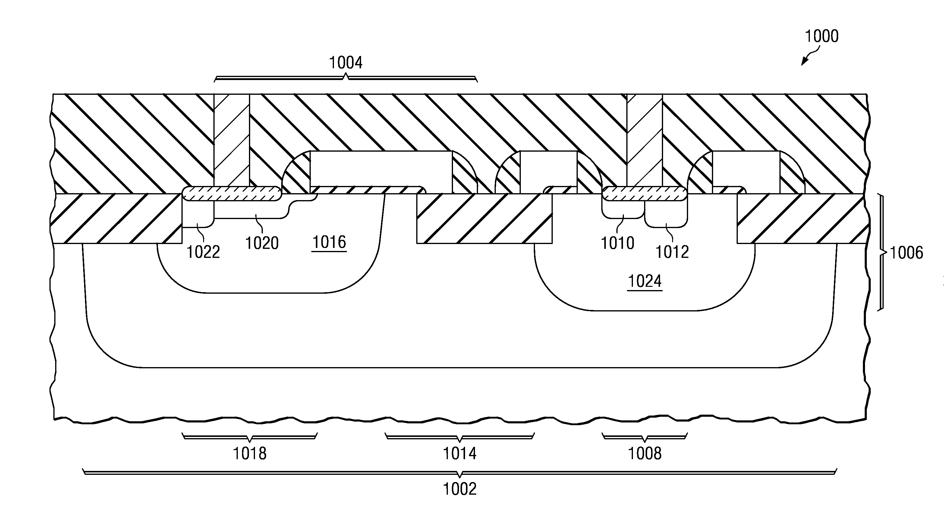
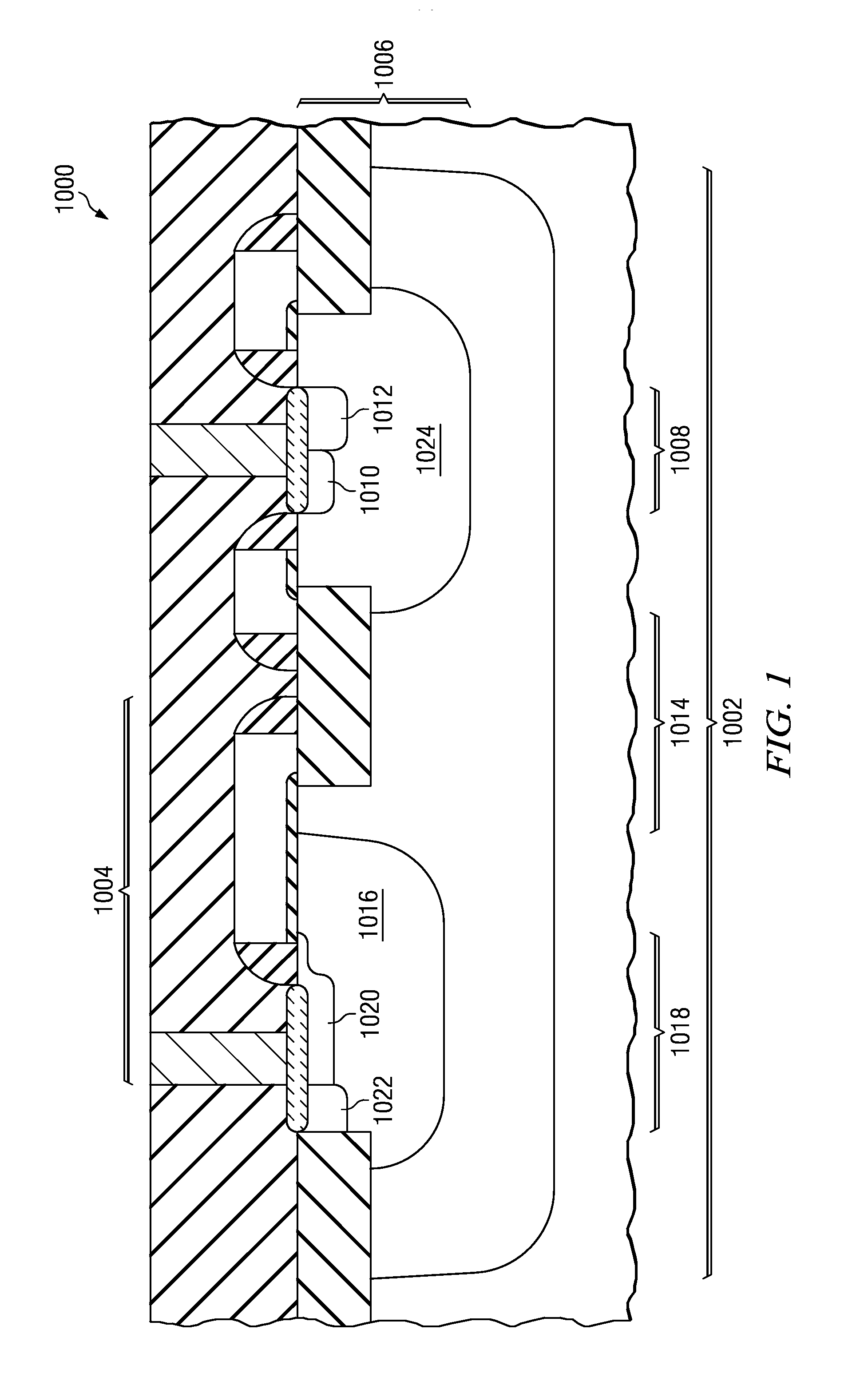
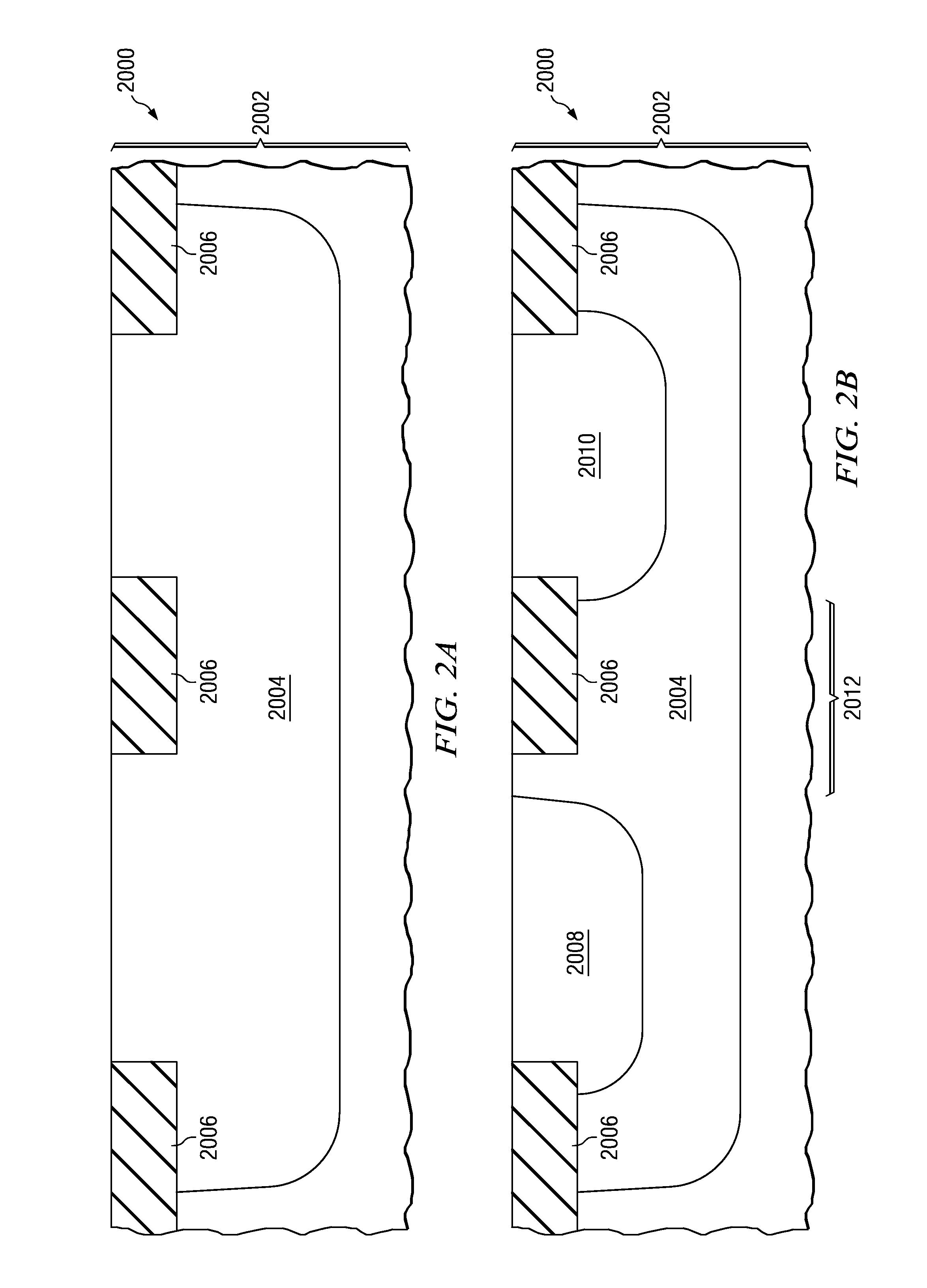
[0011]The present invention is described with reference to the attached figures, wherein like reference numerals are used throughout the figures to designate similar or equivalent elements. The figures are not drawn to scale and they are provided merely to illustrate the invention. Several aspects of the invention are described below with reference to example applications for illustration. It should be understood that numerous specific details, relationships, and methods are set forth to provide a understanding of the invention. One skilled in the relevant art, however, will readily recognize that the invention can be practiced without one or more of the specific details or with other methods. In other instances, well-known structures or operations are not shown in detail to avoid obscuring the invention. The present invention is not limited by the illustrated ordering of acts or events, as some acts may occur in different orders and / or concurrently with other acts or events. Furthe...


PUM


Abstract

An integrated circuit having an SCRMOS transistor with a RESURF region around the drain region and SCR terminal. The RESURF region is the same conductivity type as the drift region and is more heavily doped than the drift region. An SCRMOS transistor with a RESURF region around the drain region and SCR terminal. A process of forming an integrated circuit having an SCRMOS transistor with a RESURF region around the drain region and SCR terminal.

Description

[0001]The following co-pending patent application is related and hereby incorporated by reference: U.S. patent application Ser. No. 12 / ______ (Texas Instruments docket number TI-67986, filed simultaneously with this application).FIELD OF THE INVENTION[0002]This invention relates to the field of integrated circuits. More particularly, this invention relates to MOS transistors in integrated circuits.BACKGROUND OF THE INVENTION[0003]Metal oxide semiconductor (MOS) transistors integrated with silicon controlled rectifier (SCR) devices may exhibit degraded reliability from high voltage transients such as ESD events. During high voltage transients, charge carriers may be locally injected into lightly doped regions, causing a reduced voltage at the point of injection, which in turn may lead to more charge carrier injection. Localized charge carrier injection by this mechanism may cause device damage.SUMMARY OF THE INVENTION[0004]The following presents a simplified summary in order to provi...

Claims


Application Information

Patent Timeline
Patent Type & Authority Applications(United States)
IPC IPC(8): H01L27/06H01L21/8249
CPCH01L27/0262H01L29/063H01L29/0649H01L29/0692H01L29/0834H01L29/749H01L29/402H01L29/456H01L29/66393H01L29/7436H01L29/1016
Inventor PENDHARKAR, SAMEER P.
Owner TEXAS INSTR INC
Why Eureka
Try Eureka