Semiconductor device and circuit board having the semiconductor device mounted thereon

a semiconductor device and circuit board technology, applied in the field of semiconductor devices and circuit boards having the semiconductor devices mounted thereon, can solve the problems of large deviation of the impedance of the replica buffer b>130/b> at the pull-down side and the impedance of the replica buffer b>130/b> at the pull-down side is greatly deviated from the impedance of the external resistor

Inactive Publication Date: 2011-08-11
ELPIDA MEMORY INC
View PDF1 Cites 44 Cited by
  • Summary
  • Abstract
  • Description
  • Claims
  • Application Information

AI Technical Summary

Benefits of technology

[0017]According to the present invention, impedances of the first and third replica buffers are adjusted based on a potential of the first terminal, and therefore an adjustment error at the pull-up side is not superimposed with an adjustment error at the pull-down side, unlike in conventional impedance adjusting circuits. In addition, because a current mirror circuit is not used for a current source, there is no risk of occurrence of an impedance adjustment error attributable to fluctuations of a current value due to a reduced power source voltage.

Problems solved by technology

When an input / output signal has a small amplitude, the required precision of an impedance of an output buffer becomes very severe.
As a result, fluctuations occur in a current value of the current IZQ and an impedance adjustment error attributable to the variations of the current value occurs.
Consequently, there has been a risk that the impedance of the replica buffer 130 at the pull-down side is greatly deviated from the impedance of the external resistor.

Method used


Image

  • Semiconductor device and circuit board having the semiconductor device mounted thereon
  • Semiconductor device and circuit board having the semiconductor device mounted thereon
  • Semiconductor device and circuit board having the semiconductor device mounted thereon

Examples


Embodiment Construction

[0030]Preferred embodiments of the present invention will be explained below in detail with reference to the accompanying drawings.

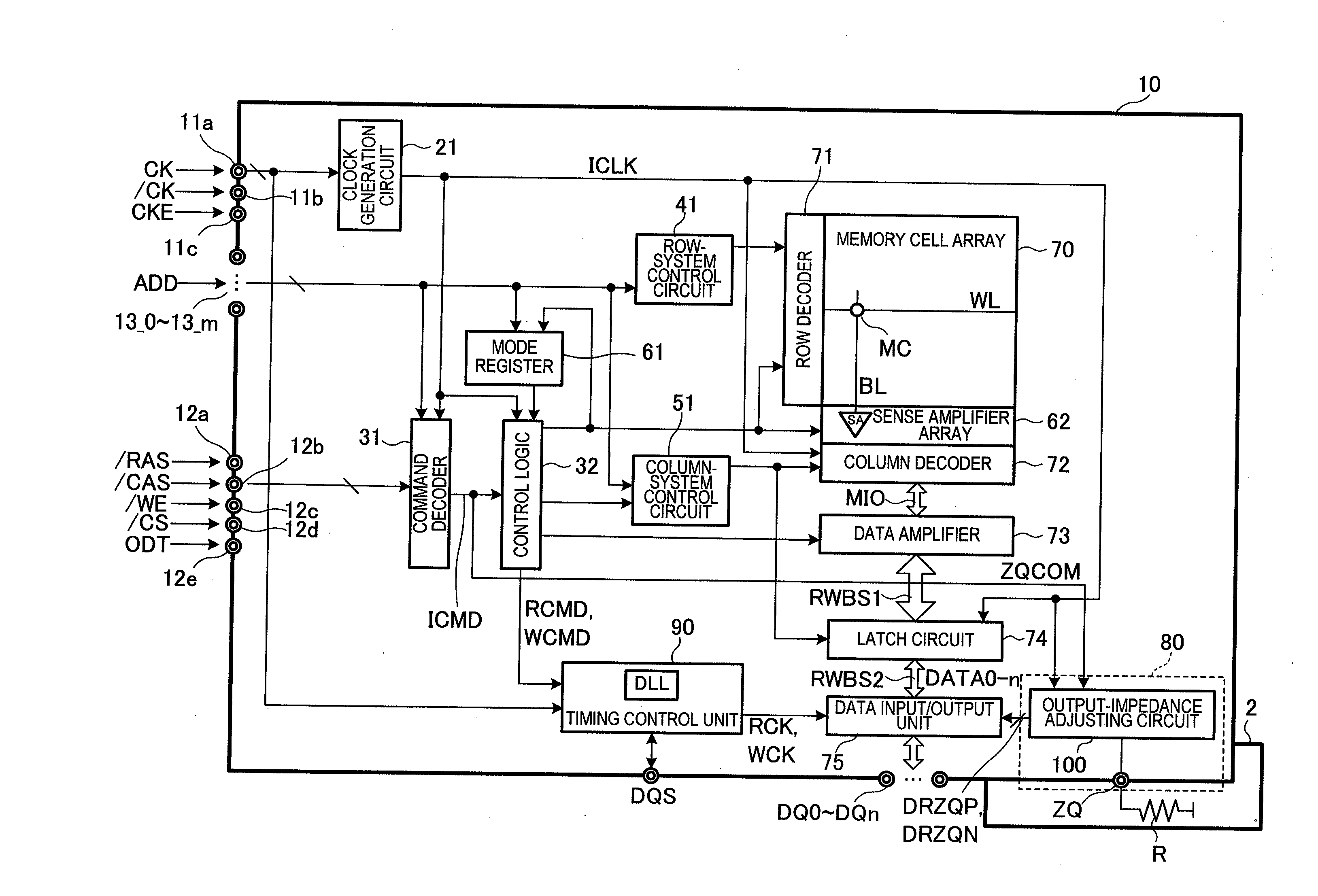
[0031]FIG. 1 is a block diagram showing a configuration of a semiconductor device according to an embodiment of the present invention.

[0032]As shown in FIG. 1, a semiconductor device 10 according to the present embodiment includes clock pads 11a and 11b, a clock enable pad 11c, command pads 12a to 12e, address pads 13_0 to 13_m, data pads DQ0 to DQn, a data strobe pad DQS, and a calibration pad ZQ as external terminals. Although the semiconductor device 10 also includes a power source pad or the like, these parts are not shown in FIG. 1.

[0033]The clock pads 11a and 11b are supplied with external clock signals CK and / CK, respectively. The clock enable pad 11c is supplied with a clock enable signal CKE. The external clock signals CK, / CK and the clock enable signal CKE supplied are supplied to a clock generation circuit 21. In the present specification, s...


PUM


Abstract

To provide a semiconductor device including a first replica buffer connected to a calibration terminal, an impedance adjusting circuit that changes an impedance of the first replica buffer according to a comparison result between a potential of the terminal and a reference potential, and an impedance adjusting circuit that changes an impedance of a third replica buffer according to a comparison result between a potential of a connection node of a second replica buffer and the third replica buffer and a potential of the terminal. According to the present invention, both impedances of the first and third replica buffers are adjusted based on the potential of the terminal, and therefore an adjustment error of one of the replica buffers is not superimposed with an adjustment error of the other replica buffer.

Description

BACKGROUND OF THE INVENTION[0001]1. Field of the Invention[0002]The present invention relates to a semiconductor device and a circuit board having the semiconductor device mounted thereon, and more particularly relates to a semiconductor device capable of adjusting an impedance of an output buffer and a circuit board having the semiconductor device mounted thereon.[0003]2. Description of Related Art[0004]In recent years, a data transfer between semiconductor devices (such as between a CPU and a memory device) requires a very high data-transfer rate. To achieve this, an amplitude of an input / output signal is made increasingly smaller. When an input / output signal has a small amplitude, the required precision of an impedance of an output buffer becomes very severe.[0005]The impedance of an output buffer not only fluctuates according to a processing condition at a time of manufacturing but also is influenced by an ambient temperature and a fluctuation of a power source voltage when the ...

Claims


Application Information

Patent Timeline
Patent Type & Authority Applications(United States)
IPC IPC(8): H03K17/16
CPCG11C7/1051G11C7/1057G11C7/1078G11C7/1084G11C7/22G11C7/222H04L25/0278G11C29/022G11C29/023G11C29/028G11C29/50008G11C2207/2254H03K19/0005G11C29/02
Inventor NAKAGAWA, HIROSHINISHIMURA, SATORU
Owner ELPIDA MEMORY INC
Why Eureka
Try Eureka