Circuit substrate

a technology of circuit substrate and circuit board, which is applied in the direction of printed circuits, electrical equipment, waveguides, etc., can solve the problems that the conventional double-layered circuit substrate design cannot meet the needs of high density and high speed wiring, and affect the wiring space available for the signal lines, so as to preserve the layout space of the signal lines, reduce the single-end impedance value, and maintain the characteristic impedance constant

Inactive Publication Date: 2011-08-18
SUNPLUS TECH CO LTD
View PDF3 Cites 6 Cited by
  • Summary
  • Abstract
  • Description
  • Claims
  • Application Information

AI Technical Summary

Benefits of technology

[0036]In summary, in a circuit substrate according to embodiments of the invention, a ground plane that requires a large area is replaced by a 3-D grounding circuit loop. Therefore, in order to preserve a layout space of the signal lines, the ground plane no longer needs to be disposed on a surface of the circuit substrate. Moreover, signal lines and adjacent ground lines may be disposed on both sides of the circuit substrate, and a trace width, a superposed thickness, and a trace thickness may be concurrently controlled, so that a characteristic impedance of the signal lines may be kept constant, and a single-end impedance value may be reduced. For example, a double-layered printed circuit board may have a single-end impedance value of 140 ohms lowered to 75 ohms, for use in high speed signals of DDRII-666 Mbps or above. Since the circuit substrate may be arranged with specialized BGA ball pads, where each one of the signal lines is substantially parallel to an adjacent ground line, a normal signal can be accurately and completely transmitted from one point of the signal line to another, so that a signal integrity is maintained.

Problems solved by technology

However, the size of an area occupied by the reference plane affects the wiring space available for the signal lines, especially for a double-layered circuit substrate.
Therefore, the conventional doubled-layered circuit substrate design cannot satisfy needs for high density and high speed wiring.

Method used


Image

  • Circuit substrate
  • Circuit substrate
  • Circuit substrate

Examples


Embodiment Construction

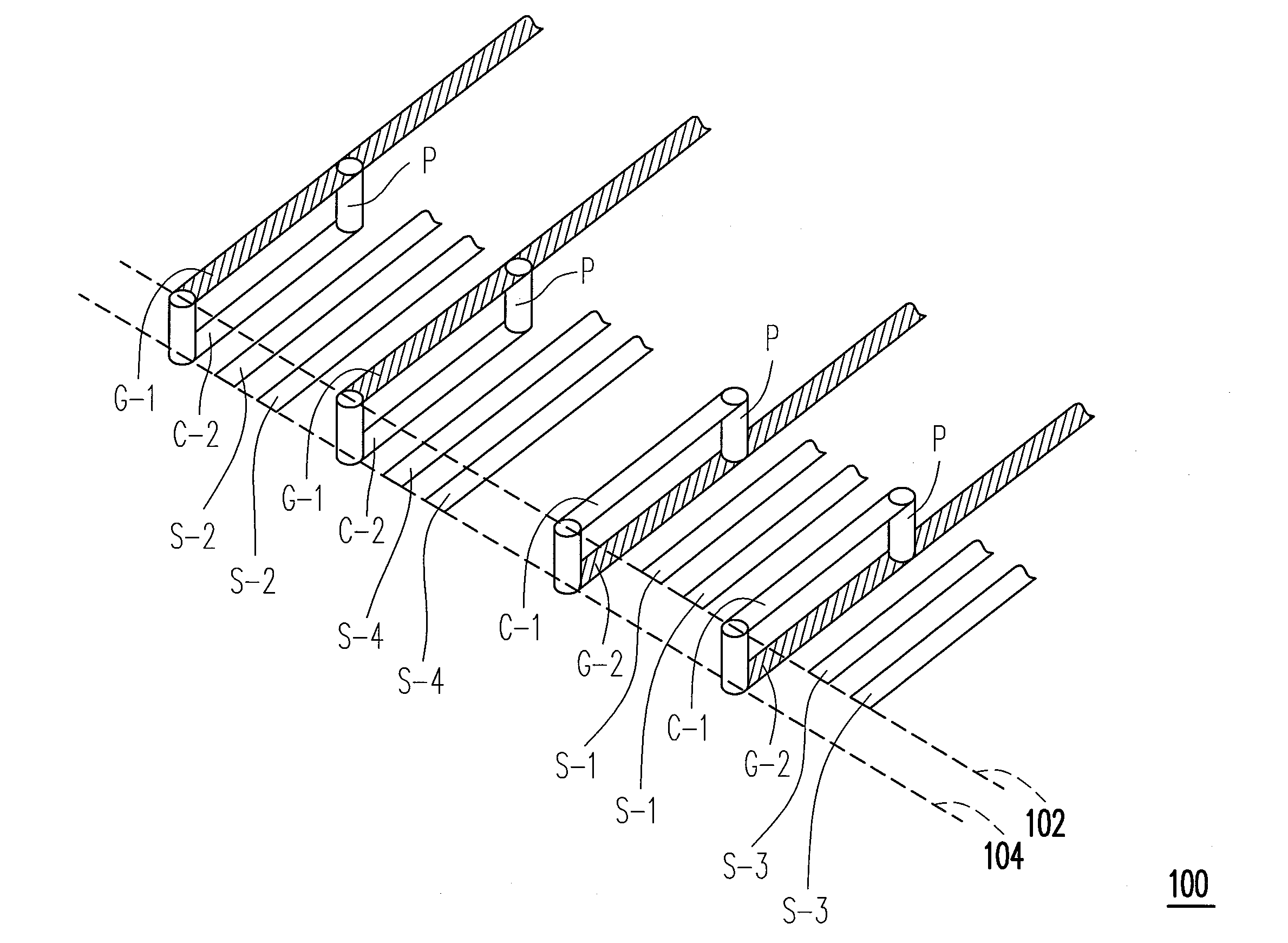
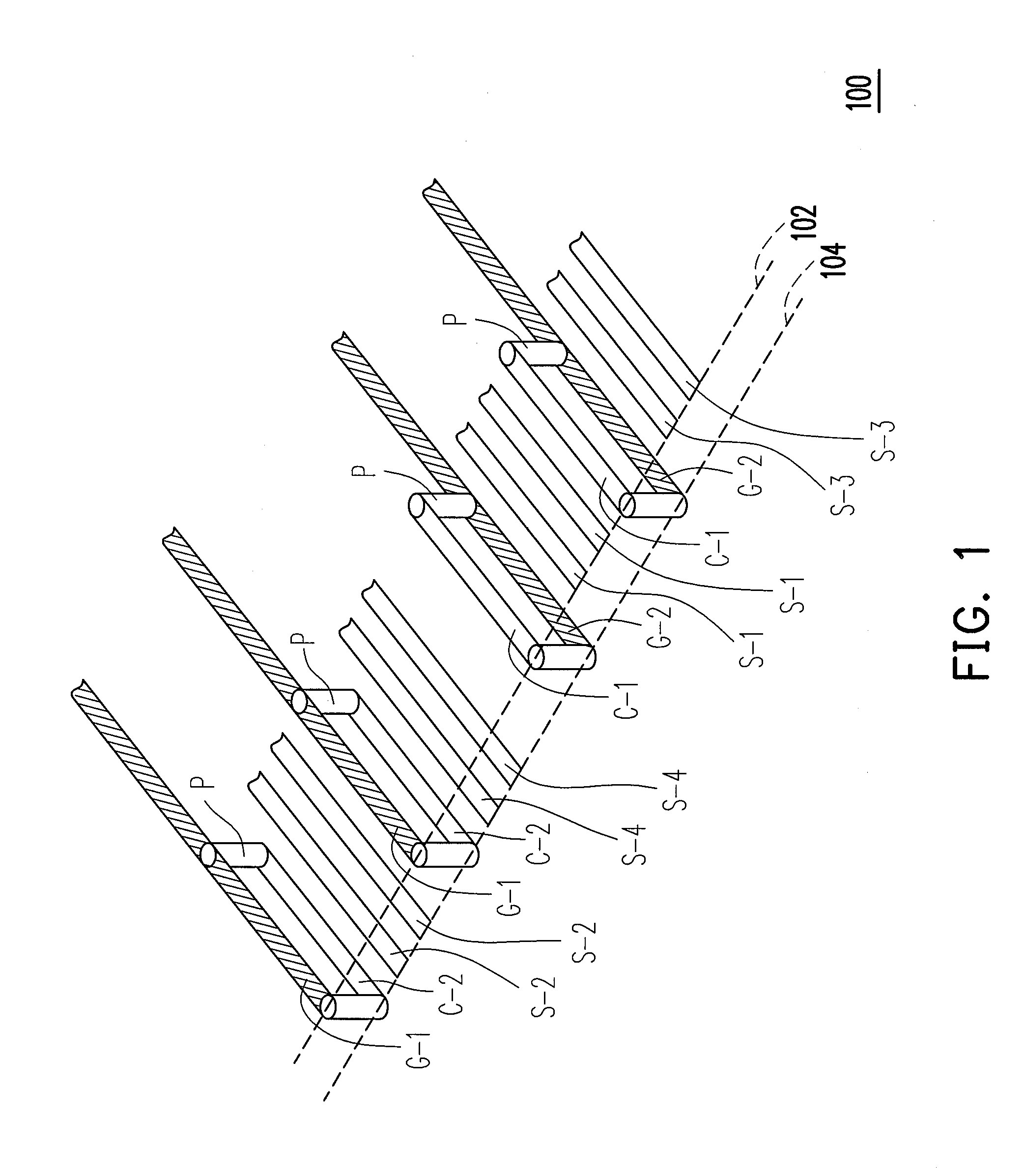
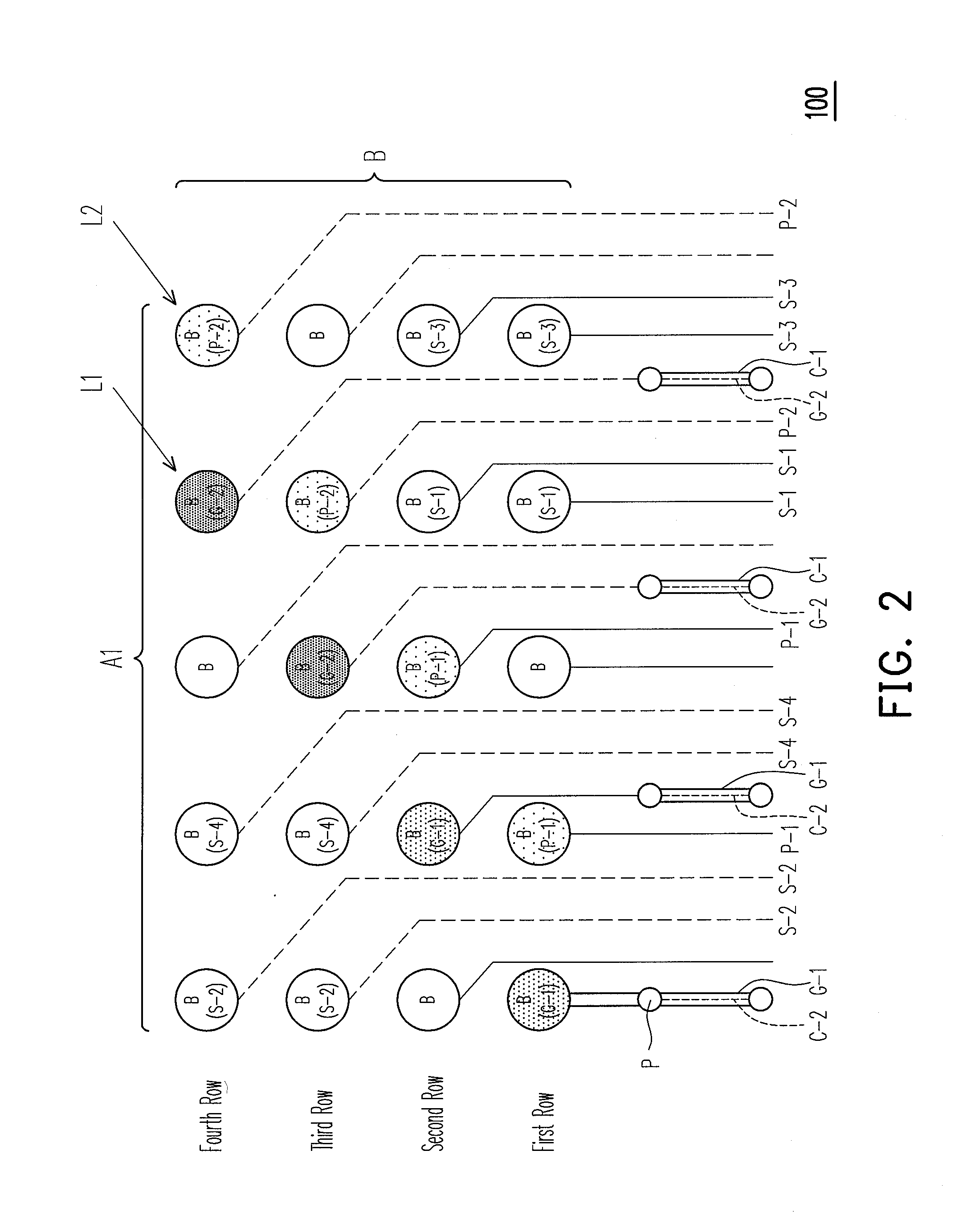
[0045]FIG. 1 is a schematic cross-sectional view of a circuit substrate structure in accordance with a first embodiment of the invention. FIG. 2 is a schematic view of a layout pattern of the circuit substrate in accordance with the first embodiment of the invention. In the embodiments described hereafter, an unit area of a circuit layout of a circuit substrate is used as an example. The unit area is defined as the smallest unit that can be repeatedly arranged with same layout.

[0046]Referring to FIG. 1, a circuit substrate 100 includes a first pair of ground lines G-1, a second pair of ground lines G-2, a plurality of first connection lines C-1 (e.g., two lines), a plurality of second connection lines C-2 (e.g., two lines), and a plurality of conductive pillars P. The first pair of ground lines G-1 is located on a first surface 102 of the circuit substrate 100. The second pair of ground lines G-2 is located on a second surface 104 of the circuit substrate 100. In the present embodim...


PUM


Abstract

A circuit substrate includes a first pair of ground lines, a second pair of ground lines, a plurality of first connection lines, a plurality of second connection lines and a plurality of conductive pillars. The first and second pairs of ground lines are located on first and second surfaces of the substrate, respecteively. The pillars are located in the substrate and vertically conducted between the first pair of ground lines and the second connection lines and between the second pair of ground lines and the first connection lines, and the first and second pairs of ground lines are conducted, so that a 3-D grounding circuit loop is formed. Moreover, a first pair of signal lines is disposed between the first connection lines for grounding and a second pair of signal lines is disposed between the second connection lines for grounding to get a better signal integrity.

Description

CROSS-REFERENCE TO RELATED APPLICATION[0001]This application claims the priority benefit of Taiwan application serial no. 99104792, filed on Feb. 12, 2010. The entirety of the above-mentioned patent application is hereby incorporated by reference herein and made a part of specification.BACKGROUND OF THE INVENTION[0002]1. Field of the Invention[0003]The invention generally relates to a circuit substrate, and more particularly, to a circuit substrate having a three-dimensional (3-D) grounding circuit loop.[0004]2. Description of Related Art[0005]In order to maintain signal integrity and power integrity, a conventional circuit substrate for transmission of high speed signals typically adopts a full reference plane. This is done so that when an electronic signal is transmitted in a signal line, a characteristic impedance of the signal line is kept constant. A good impedance matching design between a control terminal and a device terminal is crucial to reduce the insertion loss and the r...

Claims


Application Information

Patent Timeline
Patent Type & Authority Applications(United States)
IPC IPC(8): H01P3/08
CPCH05K1/025H05K2201/0979H05K2201/09672H05K2201/09354
Inventor YEH, TING-HAO
Owner SUNPLUS TECH CO LTD
Why Eureka
Try Eureka