Liquid crystal display device

a liquid crystal display and display device technology, applied in non-linear optics, instruments, optics, etc., can solve the problems of unstable border between the clockwise and the counter-clockwise area, and achieve the effect of reducing residual images and high transmittan

Active Publication Date: 2011-09-15
PANASONIC LIQUID CRYSTAL DISPLAY CO LTD +1
View PDF2 Cites 19 Cited by
  • Summary
  • Abstract
  • Description
  • Claims
  • Application Information

AI Technical Summary

Benefits of technology

[0025]According to the liquid crystal display device of the present invention, the reduction of residual images, which are generated when depression pressure is applied, and high transmittance can be both accomplished.

Problems solved by technology

At the curved portion in the stripe-patterned electrode, a change in electric field direction (orientation) is as small as 16 degrees and the change is continuous, which makes the border between the clockwise area and the counter-clockwise area very unstable.

Method used


Image

  • Liquid crystal display device
  • Liquid crystal display device
  • Liquid crystal display device

Examples


example 1

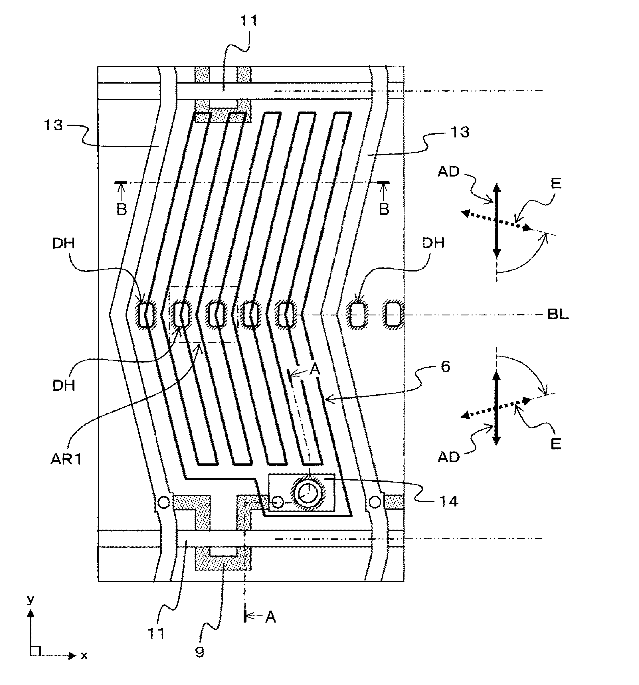
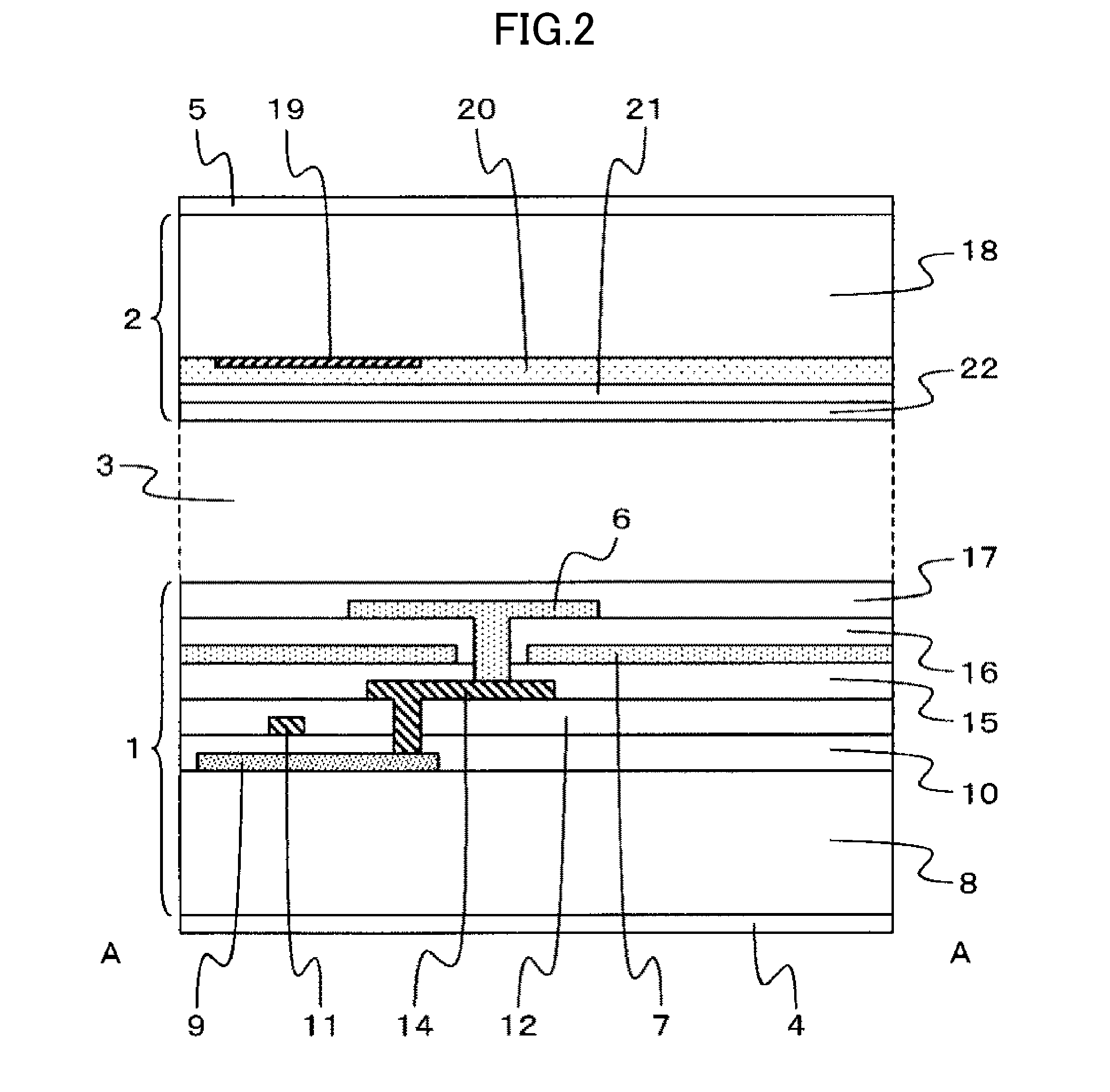
[0045]FIGS. 1 to 5 are schematic diagrams illustrating a schematic structure of a liquid crystal display panel according to Example 1 of the present invention.

[0046]FIG. 1 is a schematic plan view illustrating an example of a planar structure of a pixel in the liquid crystal display panel according to Example 1 of the present invention. FIG. 2 is a schematic sectional view illustrating an example of a sectional structure taken along the line A-A of FIG. 1. FIG. 3 is a schematic sectional view illustrating an example of a sectional structure taken along the line B-B of FIG. 1. FIG. 4 is an enlarged schematic plan view of an area AR1 of FIG. 1. FIG. 5 is a schematic sectional view illustrating an example of a sectional structure taken along the line C-C of FIG. 4.

[0047]FIG. 5 illustrates only a part of the sectional structure of the liquid crystal display panel that contains a pixel electrode and a common electrode, which are the main focus of the present invention, and their surround...

example 2

[0073]FIGS. 8 to 11 are schematic diagrams illustrating a schematic structure of a liquid crystal display panel according to Example 2 of the present invention.

[0074]FIG. 8 is a schematic plan view illustrating an example of a planar structure of a pixel in the liquid crystal display panel according to Example 2 of the present invention. FIG. 9 is a schematic sectional view illustrating an example of a sectional structure taken along the line D-D of FIG. 8. FIG. 10 is a schematic sectional view illustrating an example of the sectional structure taken along the line E-E of FIG. 8. FIG. 11 is an enlarged schematic plan view of an area AR2 of FIG. 8.

[0075]The liquid crystal display panel of Example 2 includes, for example, a first substrate 1, a second substrate 2, a liquid crystal layer 3, a first polarizing plate 4, and a second polarizing plate 5 as illustrated in FIGS. 8 to 10. A pixel electrode 6 and a common electrode 7 which are for applying an electric field to the liquid cryst...

example 3

[0088]FIG. 13 is a schematic plan view illustrating an example of a planar structure of a dot opening (dot hole) in a liquid crystal display panel according to Example 3 of the present invention.

[0089]Example 3 describes a more desirable shape of the dot holes DH that are provided in the pixel electrode 6, based on the pixel structure of Example 2.

[0090]In the liquid crystal display panel of Example 3, the dot holes DH provided in the pixel electrode 6 each have, for example, a substantially isosceles triangle shape in plan view, and the base thereof runs below the curved portion of the common electrode 7 (slip electrode portions) as illustrated in FIG. 13. In this Example, too, the dot hole DH is provided in a manner that allows only the convex one of the two outline segments of the slip electrode portion in the curved portion of the common electrode 7 to run through the dot hole area in plan view.

[0091]FIG. 14 is a schematic plan view illustrating an example of a change in liquid ...


PUM

PropertyMeasurementUnit
obtuse angleaaaaaaaaaa
electric fieldaaaaaaaaaa
distanceaaaaaaaaaa

Abstract

Provided is a liquid crystal display device that includes a liquid crystal layer sandwiched between two substrates, one of which includes a pixel electrode and a common electrode, where the electrode that is disposed closer to the liquid crystal layer has a stripe pattern that includes a plurality of slip electrode portions, and each of the plurality of slip electrode portions includes a curved portion at which each of the plurality of the slip electrode portions changes a stretching direction, and where the other electrode has a solid flat shape provided with a plurality of openings at locations that overlap with the curved portions of the plurality of slip electrode portions, the plurality of openings being provided in a manner that makes the opening in one curved portion independent and that allows only a convex outline segment of the slip electrode portion to run through an area of the opening.

Description

CROSS-REFERENCE TO RELATED APPLICATION[0001]The present application claims priority from Japanese patent application JP 2010-054613 filed on Mar. 11, 2010, the content of which is hereby incorporated by reference into this application.BACKGROUND OF THE INVENTION[0002]1. Field of the Invention[0003]The present invention relates to a liquid crystal display device and, in particular, a technology effectively applied to lateral electric field drive type liquid crystal display devices.[0004]2. Description of the Related Art[0005]In liquid crystal display devices that are mounted to cell phones, digital cameras, and the like, in recent years, resolution is increasing (the number of pixels is increasing) progressively and the areal dimensions per pixel tend to decrease accordingly. Further, the demand for high image quality is still strong in those liquid crystal display devices. Therefore, those liquid crystal display devices are required to balance high image quality and high pixel count...

Claims


Application Information

Patent Timeline
Patent Type & Authority Applications(United States)
IPC IPC(8): G02F1/1343
CPCG02F1/134363
Inventor ITOU, OSAMU
Owner PANASONIC LIQUID CRYSTAL DISPLAY CO LTD
Why Eureka
Try Eureka