Liquid crystal display panel and manufacturing method thereof

A technology of a liquid crystal display panel and a manufacturing method, which are applied in directions such as static indicators, can solve the problems affecting the reaction speed performance of the liquid crystal display panel, etc., and achieve the effects of improving display quality, low light leakage, and good display characteristics

Inactive Publication Date: 2010-04-28
CENTURY DISPLAY (SHENZHEN) CO LTD
View PDF0 Cites 14 Cited by
  • Summary
  • Abstract
  • Description
  • Claims
  • Application Information

AI Technical Summary

Problems solved by technology

[0007] It can be seen from Table 1 that in the known liquid crystal display panel, the response times of the red sub-pixel R, the green sub-pixel G, the blue sub-pixel B and the white sub-pixel W are different, which will affect the liquid crystal display panel. The overall response speed performance, what's more, it is prone to image sticking and other poor display

Method used


Image

  • Liquid crystal display panel and manufacturing method thereof
  • Liquid crystal display panel and manufacturing method thereof
  • Liquid crystal display panel and manufacturing method thereof

Examples


no. 1 example

[0034] Figure 3A to Figure 3D It is a schematic cross-sectional flow diagram of a manufacturing method of a liquid crystal display panel according to the first embodiment of the present invention.

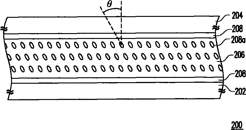
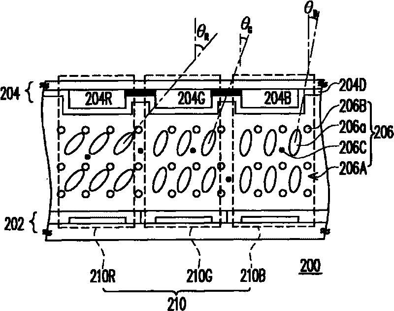
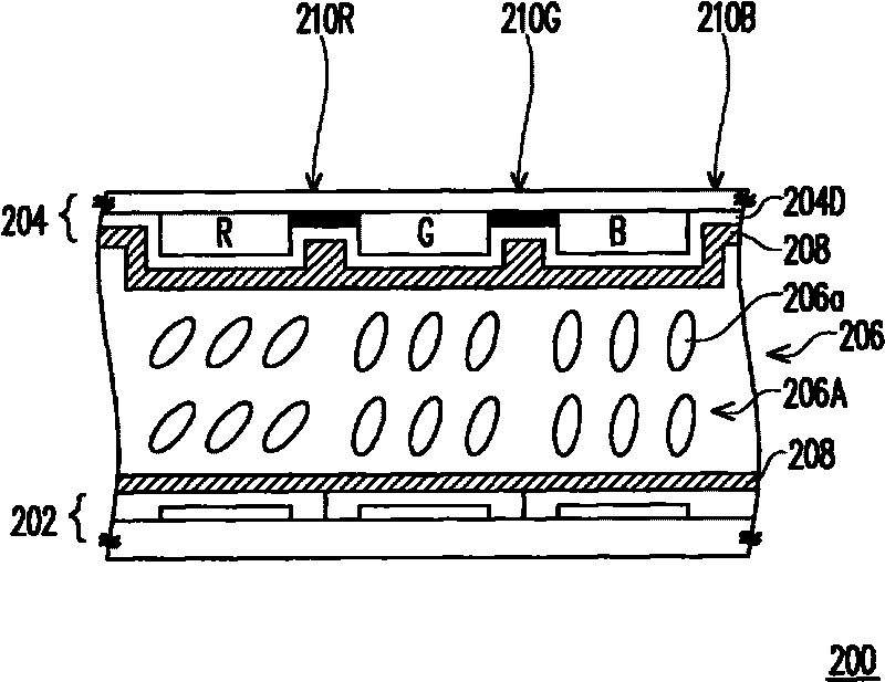
[0035] Please refer to Figure 3A Firstly, a first substrate 202 , a second substrate 204 and a liquid crystal layer 206 sealed between the first substrate 202 and the second substrate 204 are provided. The first substrate 202 is, for example, an active device array substrate, and the second substrate 204 is, for example, a color filter substrate. The first substrate 202 includes a substrate 202A, an active layer 202B and a pixel electrode layer 202C. The second substrate 204 includes a red filter layer 204R, a green filter layer 204G, a blue filter layer 204B and a common electrode 204D. The liquid crystal layer 206 includes a liquid crystal composition 206A, a photosensitive molecular monomer 206B and a photoinitiator 206C. In this way, the first substrate 202, the second su...

no. 2 example

[0041] Figure 4A to Figure 4D It is a schematic cross-sectional flow diagram of a manufacturing method of a liquid crystal display panel according to the second embodiment of the present invention. Wherein, the flow of the manufacturing method of the liquid crystal display panel 200B of this embodiment is similar to that of the first embodiment, but in the manufacturing method of the liquid crystal display panel 200A of this embodiment, it is used to drive the red sub-pixel 210R and the green sub-pixel 210G And the voltage relationship of the blue sub-pixel 210B is different.

[0042] Specifically, Figure 4A with the first embodiment Figure 3A Similar, no more details. Please refer to Figure 4B , in this embodiment, the first voltage V R , the second voltage V G , the third voltage V B For example, the following relationship is satisfied: V R >V G =V B , where the first voltage V R , the second voltage V G , the third voltage V B The range is preferably 8 volt...

no. 3 example

[0046] Figure 5A to Figure 5D It is a schematic cross-sectional flow diagram of a manufacturing method of a liquid crystal display panel according to the third embodiment of the present invention. Wherein, the flow of the manufacturing method of the liquid crystal display panel 200C of this embodiment is similar to that of the first embodiment of the liquid crystal display panel 200A, but in the manufacturing method of the liquid crystal display panel 200C of this embodiment, it is used to drive the red sub-pixel 210R, The voltage relationship between the green sub-pixel 210G and the blue sub-pixel 210B is different.

[0047] Specifically, Figure 5A with the first embodiment Figure 3A Similar, no more details. Please refer to Figure 5B , in this embodiment, the first voltage V R , the second voltage V G , the third voltage V B For example, the following relationship is satisfied: V R =V G >V B , where the first voltage V R , the second voltage V G , the third v...


PUM


Abstract

The invention provides a method for manufacturing liquid crystal display panels, comprising the following steps: providing a first substrate, a second substrate and a liquid crystal layer, wherein, the liquid crystal layer comprises a liquid crystal component, a photosensitive molecule monomer and a photoinitiator; the liquid crystal display panel is provided with a plurality of pixels, and each pixel comprises a red sub-pixel, a green sub-pixel and a blue sub-pixel, then the liquid crystal display panel controls liquid crystal component to lead a plurality of liquid crystal molecules corresponding to the red sub-pixel in the liquid crystal component to be arranged along a first pretilt angle theta R, a plurality of liquid crystal molecules corresponding to the green sub-pixel to be arranged along a second pretilt angle theta G, and a plurality of liquid crystal molecules corresponding to the blue sub-pixel to be arranged along a third pretilt theta B, and the theta G is more than or equal to the theta B and is less than or equal to theta R, and polymerizes the photosensitive molecule monomer to form a stable alignment layer of a polymer between the liquid crystal layer and the first substrate and between the liquid crystal layer and the second substrate.

Description

【Technical field】 [0001] The present invention relates to a display panel and a manufacturing method thereof, and in particular to a liquid crystal display panel and a manufacturing method thereof. 【Background technique】 [0002] The known multi-domain vertically aligned (MVA) liquid crystal display panel utilizes the configuration of an alignment structure to make the liquid crystal molecules in different regions tilt at different angles, so as to achieve the effect of wide viewing angle. The alignment structure includes alignment protrusions and alignment slits disposed on the electrodes. However, the pouring directions of the liquid crystal molecules located around the alignment bumps and the alignment slits are often discontinuous, resulting in light leakage and lowering the display contrast of the liquid crystal display panel. If in order to reduce the degree of light leakage, a light-shielding layer is disposed corresponding to the alignment bumps or alignment slits, ...

Claims


Application Information

Patent Timeline
Patent Type & Authority Applications(China)
IPC IPC(8): G02F1/133
Inventor 李得俊麦真富
Owner CENTURY DISPLAY (SHENZHEN) CO LTD
Why Eureka
Try Eureka