Wafer level image sensor packaging structure and manufacturing method of the same

Active Publication Date: 2011-10-06
TONG HSING ELECTRONICS INDS
View PDF3 Cites 13 Cited by
  • Summary
  • Abstract
  • Description
  • Claims
  • Application Information

AI Technical Summary

Benefits of technology

[0014]1. Compared with a conventional COB process, the process of the manufacturing method of the present invention is simplified and effective in dispensing with materials and reducing the height of the package structure. Thus, a wafer level image sensor package structure thus fabricated is lightweight, thin, and compact, and incurs less fabrication costs.
[0015]2. An encapsulant which is disposed along the periphery of the packaging structure not

Problems solved by technology

As a result, the image sensor packaging structure is of a relatively large size and a considerable height when packaged.
In addition, during the COB packaging period, the image sensor packaging structure is susceptible to dust intrusion or moisture permeation and thus likely to have a low conforming rate.
As a result, COB incurs high process costs.
However, conventional wafer level image sensor

Method used


Image

  • Wafer level image sensor packaging structure and manufacturing method of the same
  • Wafer level image sensor packaging structure and manufacturing method of the same
  • Wafer level image sensor packaging structure and manufacturing method of the same

Examples


Embodiment Construction

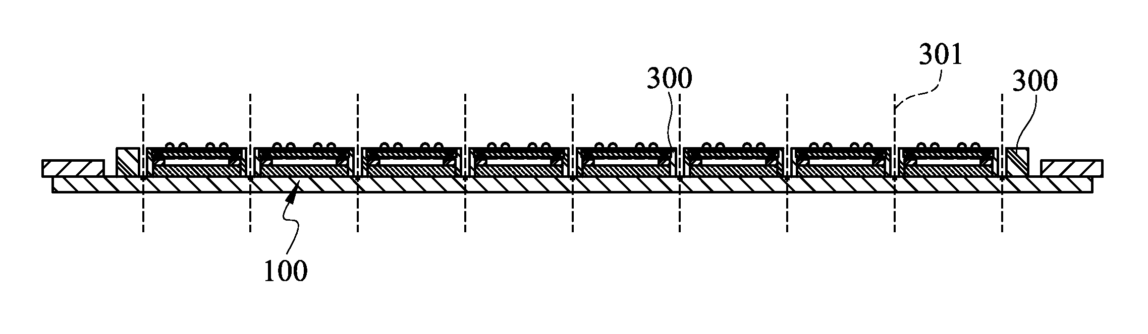
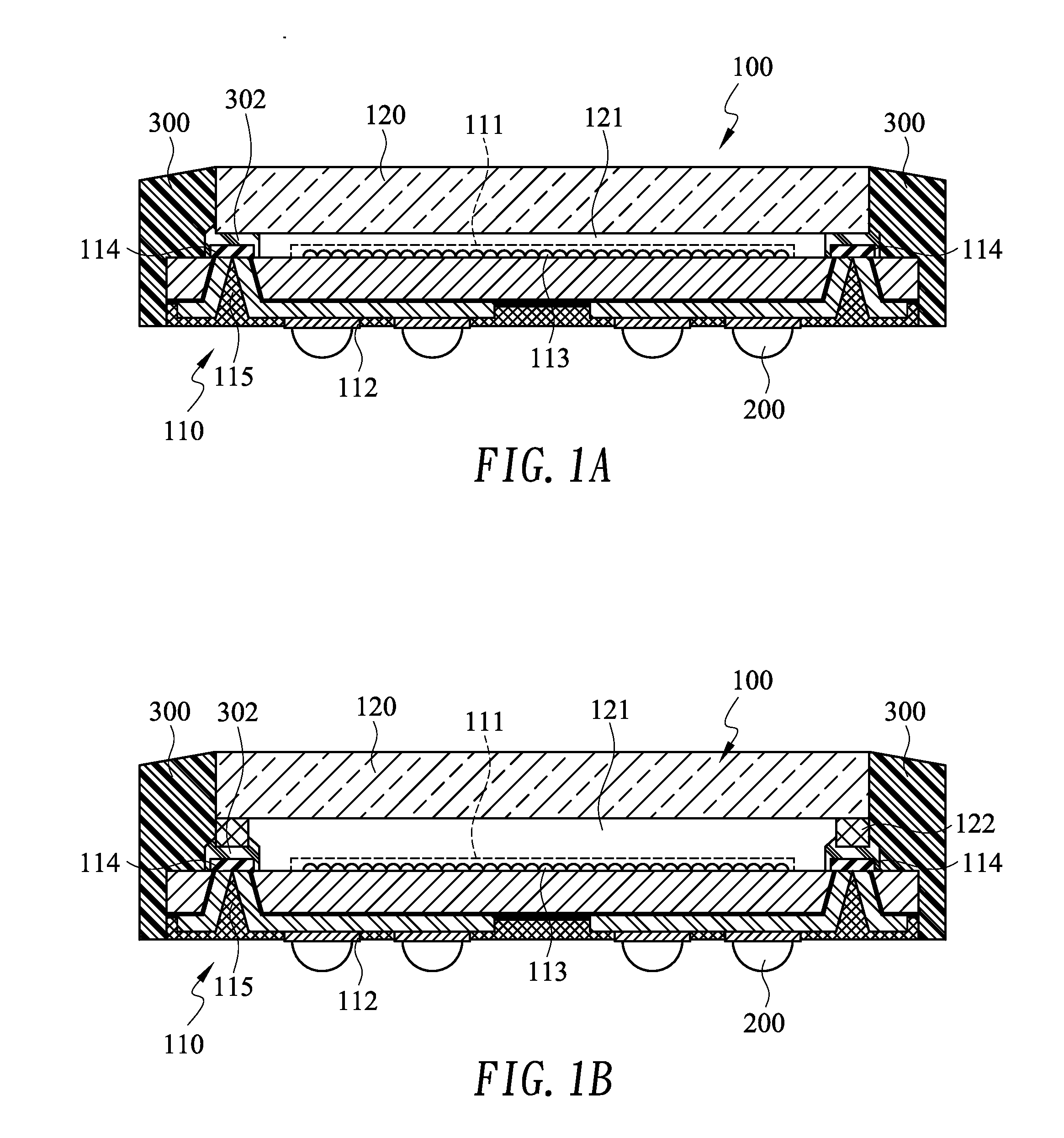
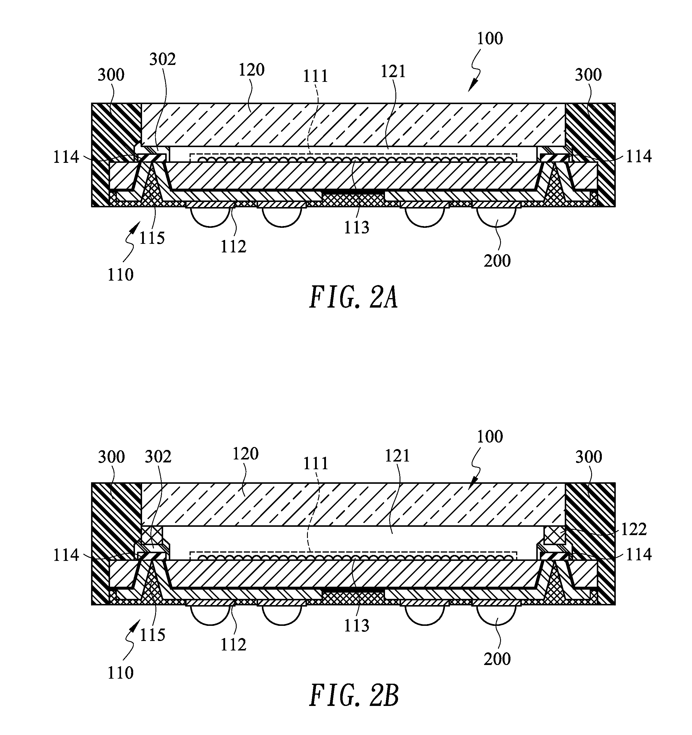
[0044]Referring to FIG. 1A through FIG. 2B, there are shown schematic views of a wafer level image sensor packaging structure according to an embodiment of the present invention. Referring to FIG. 3, there is shown a schematic perspective view of a transparent lid 120 with a supporting frame 122 thereon according to an embodiment of the present invention.

[0045]Referring to FIG. 4, there is shown a flow chart of a wafer level image sensor packaging structure manufacturing method according to an embodiment of the present invention. Referring to FIG. 5, there is shown a schematic view of a silicon wafer 101 having image sensing chips 110 according to an embodiment of the present invention. Referring to FIG. 6, there is shown a schematic view of a transparent panel 123 according to an embodiment of the present invention. Referring to FIG. 7, there is shown a schematic perspective view of a transparent lid 120 with a gridded frame thereon according to an embodiment of the present inventi...


PUM


Abstract

The present invention discloses a wafer level image sensor packaging structure and a manufacturing method of the same. The manufacturing method includes the following steps: providing a silicon wafer, dicing the silicon wafer, providing a plurality of transparent lids, fabricating a plurality of semi-finished products, performing a packaging process, mounting solder balls, and cutting an encapsulant between the semi-finished products. The manufacturing method of the invention has the advantage of being straightforward, uncomplicated, and cost-saving. Thus, the wafer level image sensor package structure is lightweight, thin, and compact. To prevent the image sensor chip from cracking on impact during handling, the encapsulant will be arranged on the lateral sides of the semi-finished products during the packaging process.

Description

BACKGROUND OF THE INVENTION[0001]1. Field of the Invention[0002]The present invention relates to wafer level image sensor packaging structures and manufacturing methods of the same, and more particularly, to a wafer level image sensor packaging structure and a manufacturing method of the same applicable to batch fabrication of the image sensor packaging structure.[0003]2. Description of Related Art[0004]In recent years, digital imaging electronic products are becoming more popular. Camera cell phones, digital cameras, and digital video recorders have evolved into such a generation that they have become indispensable to every person. Given the increasing demand for imaging electronic products, it is easy to conceive the rapid speed at which the image sensor market expands.[0005]Among the conventional methods for packaging image sensors are two predominant ones, namely Chip On Board (COB) and Chip Scale Package (CSP). In COB, an image sensing chip is adhesively attached to a substrate...

Claims


Application Information

Patent Timeline
IPC IPC(8): H01L31/0224H01L31/18H01L31/0203
CPCH01L27/14618H01L27/14687H01L27/14683H01L24/97H01L2224/13H01L2924/181H01L2924/00
Inventor TU, HSIU-WENHSIN, CHUNG-HSIENCHEN, HAN-HSINGCHEN, MING-HUIKUO, REN-LONGHSU, CHIH-CHENGSHIAO, YOUNG-HOUNGCHEN, TSAO-PIN
Owner TONG HSING ELECTRONICS INDS
Why Eureka
Try Eureka