Fringe field switching mode liquid crystal display and manufacturing method thereof

a liquid crystal display and switching mode technology, applied in the manufacture of electric discharge tubes/lamps, basic electric elements, instruments, etc., can solve the problems of poor outdoor readability, high power consumption, no use, and it is almost impossible to read information from the lcd. to achieve the effect of reducing light leakage and coupling phenomena

Active Publication Date: 2011-10-06
HYDIS TECH CO LTD
View PDF3 Cites 7 Cited by
  • Summary
  • Abstract
  • Description
  • Claims
  • Application Information

AI Technical Summary

Benefits of technology

[0015]In consideration of the above problems, it is an object of the present invention to provide a fringe field switching (FFS) mode liquid crystal display (LCD) and a manufacturing method thereof, in which outdoor readability is enhanced using basic properties of the FFS mode LCD without largely changing a process of a general transmissive FFS mode LCD.
[0016]It is another object of the present invention to provide a fringe field switching (FFS) mode liquid crystal display (LCD), in which an aperture ratio is enhanced and light leakage and coupling effect are minimized, thus improving picture quality.
[0017]It is still another object of the present invention to provide a fringe field switching (FFS) mode liquid crystal display (LCD), of which internal reflection is increased.
[0018]It is yet another object of the present invention to provide a fringe field switching (FFS) mode liquid crystal display (LCD), which has a higher aperture ratio than the conventional transmissive FFS mode LCD, thereby reducing power consumption.
[0019]In order to achieve the above objects, according to one aspect of the present invention, a fringe field switching mode liquid crystal display comprising a lower substrate, an upper substrate, and a liquid crystal layer interposed between the lower and upper substrates, in which a gate line and a data line intersect each other and define a pixel area on the lower substrate and a switching element is provided at an intersection between the gate line and the data line, comprises: a transparent common electrode having a predetermined shape and formed within the pixel area to adjust light transmittance by applying a voltage to the liquid crystal layer; and a transparent pixel electrode comprising a plurality of slits and formed above the transparent common electrode with an insulating layer interposed between the transparent common electrode and the transparent pixel electrode, wherein a rubbing direction for aligning the liquid crystal layer ranges within 5° with respect to a direction of the gate line, arrangement between the transparent common electrode and the transparent pixel electrode is regulated with respect to the data line to reduce light leakage and coupling phenomena without a light shielding region above the data line, and one end of the transparent common electrode is arranged between the data line and the transparent pixel electrode.
[0022]According to yet another aspect of the present invention, a method of manufacturing a fringe field switching mode liquid crystal display comprising a lower substrate, an upper substrate, and a liquid crystal layer interposed between the lower and upper substrates, in which a gate line and a data line intersect each other and define a pixel area on the lower substrate and a switching element is provided at an intersection between the gate line and the data line, comprises: forming a transparent common electrode on the substrate; sequentially forming the gate line, a gate insulating layer, an active layer, the data line, an interlayer insulating layer and a transparent pixel electrode having a plurality of slits on the transparent common electrode; and applying and rubbing an alignment layer for aligning the liquid crystal layer on the transparent pixel electrode, wherein arrangement between the transparent common electrode and the transparent pixel electrode is regulated with respect to the data line to reduce light leakage and coupling phenomena without a light shielding region above the data line, one end of the transparent common electrode is arranged between the data line and the transparent pixel electrode, and a ratio (L3 / L1) of a distance (L1) between the data line and the transparent pixel electrode to a distance (L3) between the data line and the transparent common electrode is within 0.75.

Problems solved by technology

The transmissive LCD uses the backlight as a light source, so that it can display an image brightly even in dark surroundings but the backlight causes high power consumption and bad outdoor readability.
On the other hand, the reflective LCD uses its surrounding natural light without the backlight, so that it can consume less power and be used in the outdoor place but it is of no use when the surroundings are dark.
In other words, the general transmissive LCD is excellent in brightness, color reproduction, contrast ration (CR), etc. as to an indoor place, but it is almost impossible to read information from the LCD because of sunlight or reflected sunlight as to the outdoor place.
Due to the sunlight stronger than one hundred thousand LUX in the outdoor place, the transmissive LCD which cannot emit light by itself is deteriorated in the outdoor readability because it depends on the brightness of the backlight and the transmittance of an LCD panel.
To solve this problem, it is possible to increase the brightness of the backlight, but too much power consumption is required.
However, when the semi-transmissive LCD is manufactured in the single cell gap structure using the same liquid crystal mode, a phase lag of the reflective region is twice that of the transmissive region, so that a voltage-reflective (V-R) curve of a reflective mode is not matched with a voltage-transmittance (V-T) curve of a transmissive mode, thereby causing inharmonious gradation and deteriorating electro-optical properties.
However, if the semi-transmissive LCD is manufactured with the dual cell gap structure, stepped difference due to the cell gap between the reflective regions increases twice, so that there are difficulties in a manufacturing process, for example, non-uniform liquid crystal alignment or the like, thereby lowering productivity.
Further, the semi-transmissive LCD shows a remarkably reduction in aperture ratio at the indoor place as well as its manufacturing process is complicated and difficult.
The resin process is difficult because it cannot perfectly avoid basic contamination on the manufacturing process, and is expensive.
In other words, cost and time for development are much required.

Method used


Image

  • Fringe field switching mode liquid crystal display and manufacturing method thereof
  • Fringe field switching mode liquid crystal display and manufacturing method thereof
  • Fringe field switching mode liquid crystal display and manufacturing method thereof

Examples


Embodiment Construction

[0032]Now, a preferred embodiment of the present invention will be described in detail with reference to the accompanying drawings.

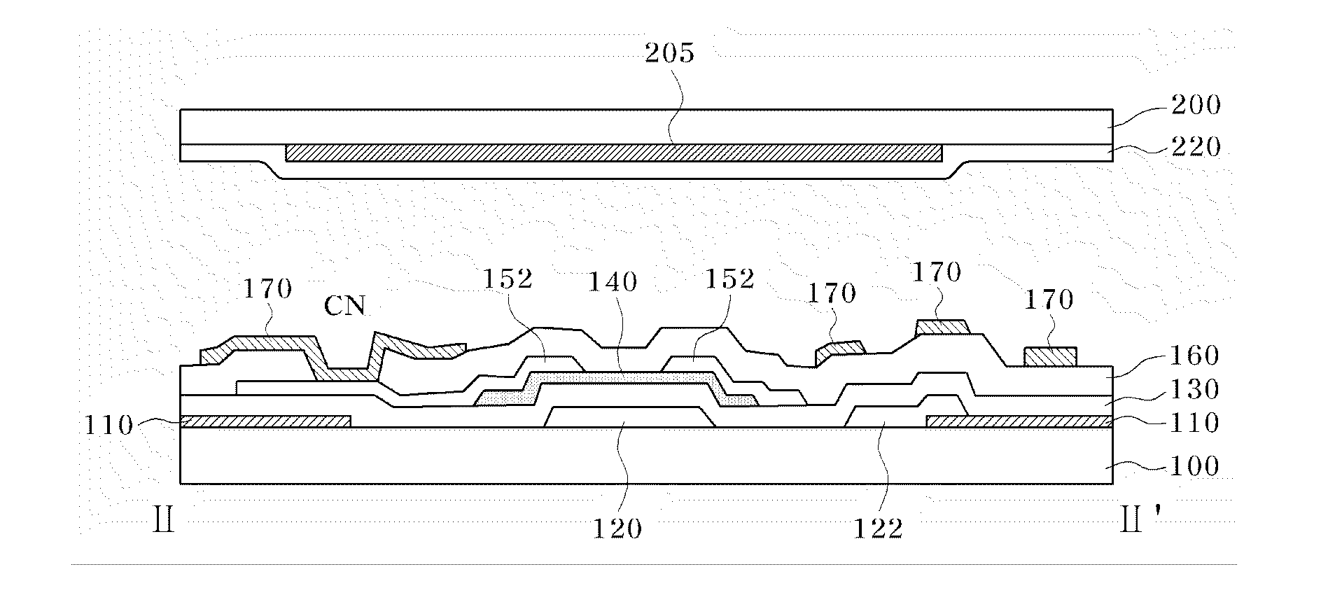
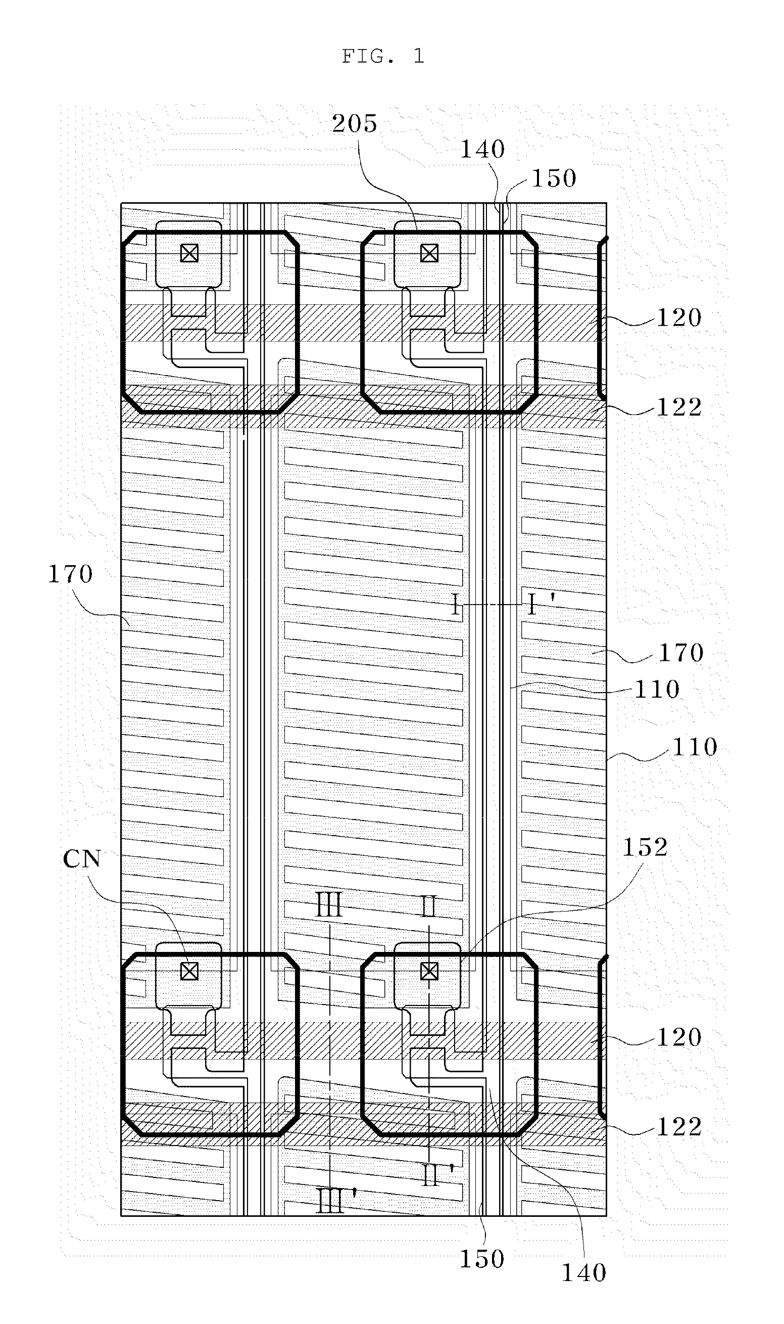
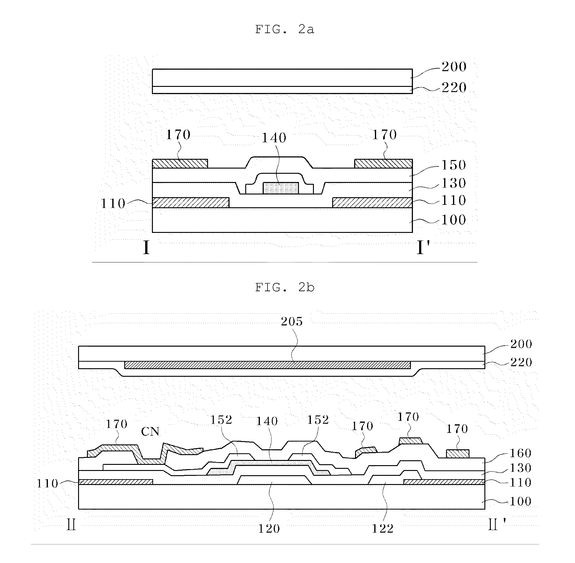
[0033]A liquid crystal display (LCD) according to an exemplary embodiment of the present invention includes a lower substrate, an upper substrate, and a liquid crystal layer interposed between the lower and upper substrates. In the lower substrate, electrodes intersect each other to apply a voltage to the liquid crystal layer, and pixels are defined by the electrodes. FIG. 1 is a partial plan view of a pixel area formed in a lower substrate of a liquid crystal display according to an exemplary embodiment of the present invention. FIGS. 2A through 2C are cross-sectional views taken along lines I-I′, II-II′ and III-III′ of FIG. 1, respectively.

[0034]Referring to FIGS. 1, 2A, 2B and 2C, in the FFS mode LCD according to an exemplary embodiment of the present invention, a gate line 120 and a data line 150 are arranged to intersect each other on a lower substr...


PUM


Abstract

Provided is a fringe field switching mode liquid crystal display. The fringe field switching mode liquid crystal display includes a transparent common electrode having a predetermined shape and formed within the pixel area to adjust light transmittance by applying a voltage to the liquid crystal layer, and a transparent pixel electrode having a plurality of slits and formed above the transparent common electrode with an insulating layer interposed between the transparent common electrode and the transparent pixel electrode. A rubbing direction for aligning the liquid crystal layer is within 5° with respect to a direction of the gate line to remove a light shielding region above the data line, one end of the transparent common electrode is arranged between the data line and the transparent pixel electrode, and a distance between the transparent common electrode and the transparent pixel electrode is regulated with respect to the data line.

Description

CROSS REFERENCE TO RELATED APPLICATIONS[0001]This application is a divisional of U.S. patent application Ser. No. 11 / 725,952, filed on Mar. 20, 2007, which is hereby incorporated by reference in its entirety.BACKGROUND OF THE INVENTION[0002]1. Field of the Invention[0003]The present invention relates to a fringe field switching (FFS) mode liquid crystal display and a manufacturing method thereof, in which an aperture ratio is improved to decrease power consumption and internal reflection is increased to enhance outdoor readability.[0004]2. Description of the Related Art[0005]A fringe field switching (FFS) mode liquid crystal display (LCD) has been proposed to improve low aperture and transmittance of an in plane switching (IPS) mode LCD.[0006]In the FFS mode LCD, a common electrode and a pixel electrode are made of a transparent conductive layer such as indium tin oxide (ITO) or the like to thereby improve its aperture ratio and transmittance as compared with the IPS mode LCD, and a...

Claims


Application Information

Patent Timeline
Patent Type & Authority Applications(United States)
IPC IPC(8): H01J9/24
CPCG02F1/133555G02F1/13378G02F2001/134372G02F1/136286G02F2001/134318G02F1/134336G02F1/134372G02F1/1343
Inventor CHOI, SUKBAEK, SEUNG JUNJANG, SOON JUJUN, TAE HYUNKIM, HYANG YUL
Owner HYDIS TECH CO LTD
Why Eureka
Try Eureka