Nonvolatile memory device having a transistor connected in parallel with a resistance switching device

a resistance switching device and memory device technology, applied in the field of nonvolatile memory devices, can solve the problems of increasing process costs, increasing bit costs using this approach, and insufficient capacity to simply increase capacity

Active Publication Date: 2011-11-24
MACRONIX INT CO LTD
View PDF1 Cites 27 Cited by
  • Summary
  • Abstract
  • Description
  • Claims
  • Application Information

AI Technical Summary

Benefits of technology

[0008]Memory devices and methods associated with memory devices are described herein. According to one aspect of the present disclosure, a memory device can comprise an array of memory cells, where each memory cell respectively comprises a transistor and a resistance switching device connected in parallel with the transistor. The transistor and the resistance switching device can each be capable of independently storing one or more bits of data. The transistor can comprise a first terminal, a second terminal, and a gate terminal, and be configured to be switchable between a plurality of different threshold voltages associated with respective memory states. The resistance switching device can be connected in parallel with the transistor such that the resistance switching device is connected to the first and second terminals of the transistor. The resistance switching device can be configured to be switchable between a plurality of different resistances associated with respective memory states.
[0009]According to another aspect of the present disclosure, a memory device can comprise a plurality of bit lines, a plurality of word lines, a first memory string comprising a first group of memory cells, and a second memory string comprising a second group of memory cells. The first and second memory strings can be connected to a common source line and to respective bit lines. The word lines can be connected to respective memory cells of the first group of memory cells and to respective memory cells of the second group of memory cells. Each of the memory cells can respectively comprise a transistor and a resistance switching device connected in parallel with the transistor. The transistor and the resistance switching device can each be capable of independently storing one or more bits of data. The transistor can comprise a first terminal, a second terminal, and a gate terminal. The transistor can be configured to be switchable between a plurality of different threshold voltages associated with respective memory states. The resistance switching device connected in parallel with the first transistor can be connected to the first and second terminals of the first transistor. The resistance switching device can be configured to be switchable between a plurality of different resistances associated with respective memory states.
[0010]According to still further aspects of the present disclosure, methods of reading and writing to a memory cell is provided for reading and writing to a memory cell that comprises a transistor and a resistance switching device connected in parallel with the transistor, where the transistor and the resistance switching device are each capable of independently storing one or more bits of data. For example, according to one aspect of the present disclosure, a reading method can comprise detecting a threshold voltage of the transistor of the memory cell, where the transistor is configured to be switchable between a plurality of threshold voltages associated with respective memory states. The reading method can also comprise detecting a resistance of the resistance switching device of the memory cell, where the resistance switching device is configured to be switchable between a plurality of resistances associated with respective memory states. These and other features, aspects, and embodiments of the invention are described below in the section entitled “Detailed Description.”

Problems solved by technology

However, it is not sufficient to simply increase capacity—it is often equally desirable to maintain, or even reduce, the size of a memory device while increasing the data storage capacity.
Still another consideration is cost.
However, some projections indicate that bit cost will begin to increase using this approach in the future, because at some point the process cost will likely begin to increase more rapidly than the memory-cell-reduction rate.

Method used


Image

  • Nonvolatile memory device having a transistor connected in parallel with a resistance switching device
  • Nonvolatile memory device having a transistor connected in parallel with a resistance switching device
  • Nonvolatile memory device having a transistor connected in parallel with a resistance switching device

Examples


Embodiment Construction

.”

BRIEF DESCRIPTION OF THE DRAWINGS

[0011]Features, aspects, and embodiments of the inventions are described in conjunction with the attached drawings, in which:

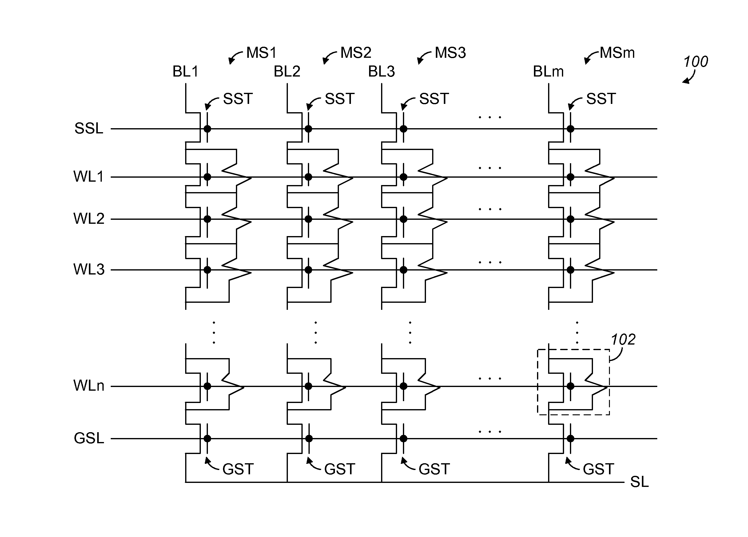
[0012]FIG. 1 shows a block diagram of a memory device in accordance with an embodiment of the present disclosure;

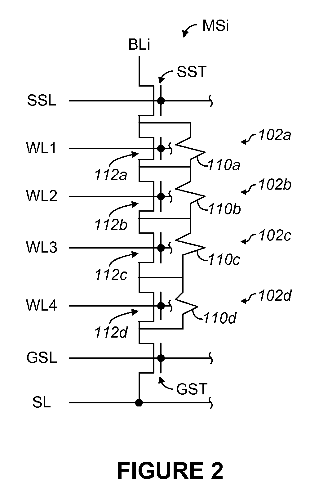
[0013]FIG. 2 shows a schematic diagram of a memory string of the memory device shown in FIG. 1;

[0014]FIG. 3 shows a schematic diagram of a memory cell of the memory device shown in FIG. 1;

[0015]FIGS. 4A and 4B show schematic views of a resistance switching device according to some embodiments of the resistance switching device shown in FIG. 3; and

[0016]FIGS. 5A-5E show resistance switching characteristics of a symmetrical two-state embodiment of the resistance switching device shown in FIGS. 4A and 4B;

[0017]FIG. 6 shows a graphical representation of relationships between the memory states of, and applied voltages to, a symmetrical two-state embodiment of the resistance switching device shown in FIGS. 4A and 4B;

[001...


PUM


Abstract

A memory device comprises an array of memory cells each capable of storing multiple bits of data. The memory cells are arranged in memory strings that are connected to a common source line. Each memory cell includes a programmable transistor connected in parallel with a resistance switching device. The transistor is switchable between a plurality of different threshold voltages associated with respective memory states. The resistance switching device is configured to be switchable between a plurality of different resistances associated with respective memory states.

Description

BACKGROUND[0001]1. Technical Field[0002]The present invention relates to electronic memory devices, and more particularly, to semiconductor memory devices suitable for use as a nonvolatile memory devices.[0003]2. Related Art[0004]Electronic memory devices are well known and commonly found in a variety of electronic systems. For example, electronic memory devices (sometimes referred to as computer memory) can be found in computers and other computing devices. Various removable or stand-alone electronic memory devices are also known, such as memory cards or solid-state data storage systems. For example, it is known to use a removable memory card for storing pictures on a digital camera or for storing movies recorded with a digital video recorder.[0005]Most electronic memory devices can be classified as either volatile or nonvolatile. A volatile electronic memory device is, in general, one which requires power in order to maintain the stored information. An example of a volatile electr...

Claims


Application Information

Patent Timeline
Patent Type & Authority Applications(United States)
IPC IPC(8): G11C11/00G11C7/00G11C7/22
CPCG11C8/14G11C11/56G11C11/5678G11C11/5685G11C13/0002G11C13/0004G11C2213/79G11C13/0009G11C13/003G11C13/004G11C13/0069G11C2013/0076G11C2213/75G11C13/0007
Inventor CHEN, YI-CHOUCHIEN, WEI-CHIHLEE, FENG-MING
Owner MACRONIX INT CO LTD
Why Eureka
Try Eureka