Process for Forming FINS for a FinFET Device

a technology of field effect transistors and fins, which is applied in the field of multi-gate field effect transistors (fets), can solve the problems of increasing device power consumption, reaching their limits, and devices often having poor thermal properties

Active Publication Date: 2012-02-02
ADVANCED MICRO DEVICES INC
View PDF5 Cites 58 Cited by
  • Summary
  • Abstract
  • Description
  • Claims
  • Application Information

AI Technical Summary

Problems solved by technology

However, at the current pace of device scaling, it is predicted that planar transistors will soon reach their limits, in terms of minimize size.
Further, as these devices get smaller, they increasingly suffer from undesirable short channel effects, such as off-state leakage current, which increases power consumption by the device.
However, such devices often have poor thermal properties, e.g., poor heat dissipation, as well as relatively significant external resistances.

Method used


Image

  • Process for Forming FINS for a FinFET Device
  • Process for Forming FINS for a FinFET Device
  • Process for Forming FINS for a FinFET Device

Examples


Embodiment Construction

[0039]The following detailed description is of example embodiments of the presently claimed invention with references to the accompanying drawings. Such description is intended to be illustrative and not limiting with respect to the scope of the present invention. Such embodiments are described in sufficient detail to enable one of ordinary skill in the art to practice the subject invention, and it will be understood that other embodiments may be practiced with some variations without departing from the spirit or scope of the subject invention.

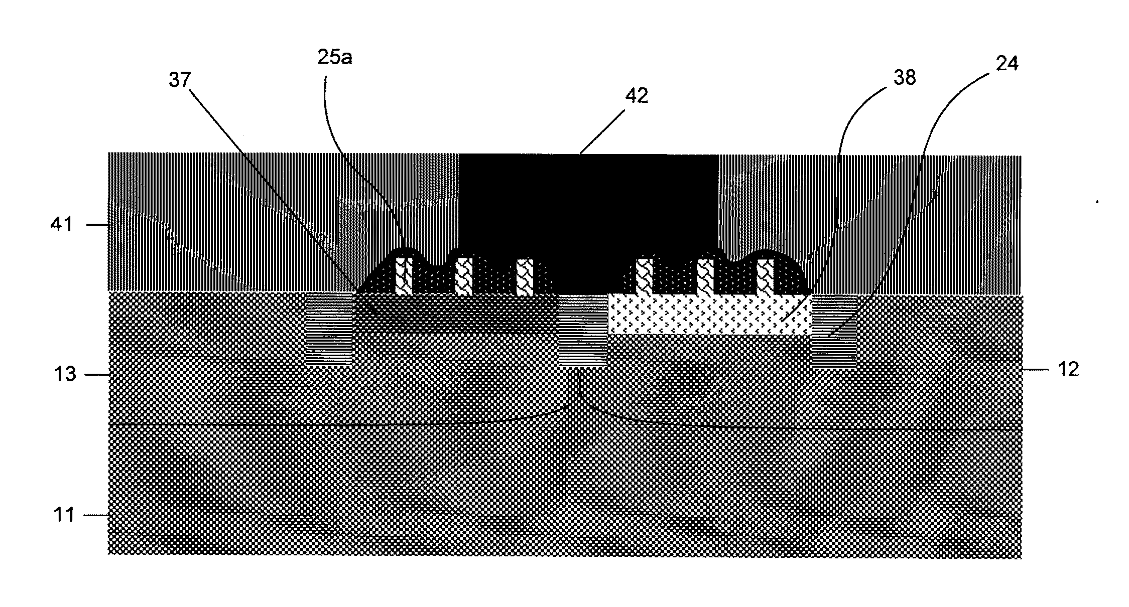
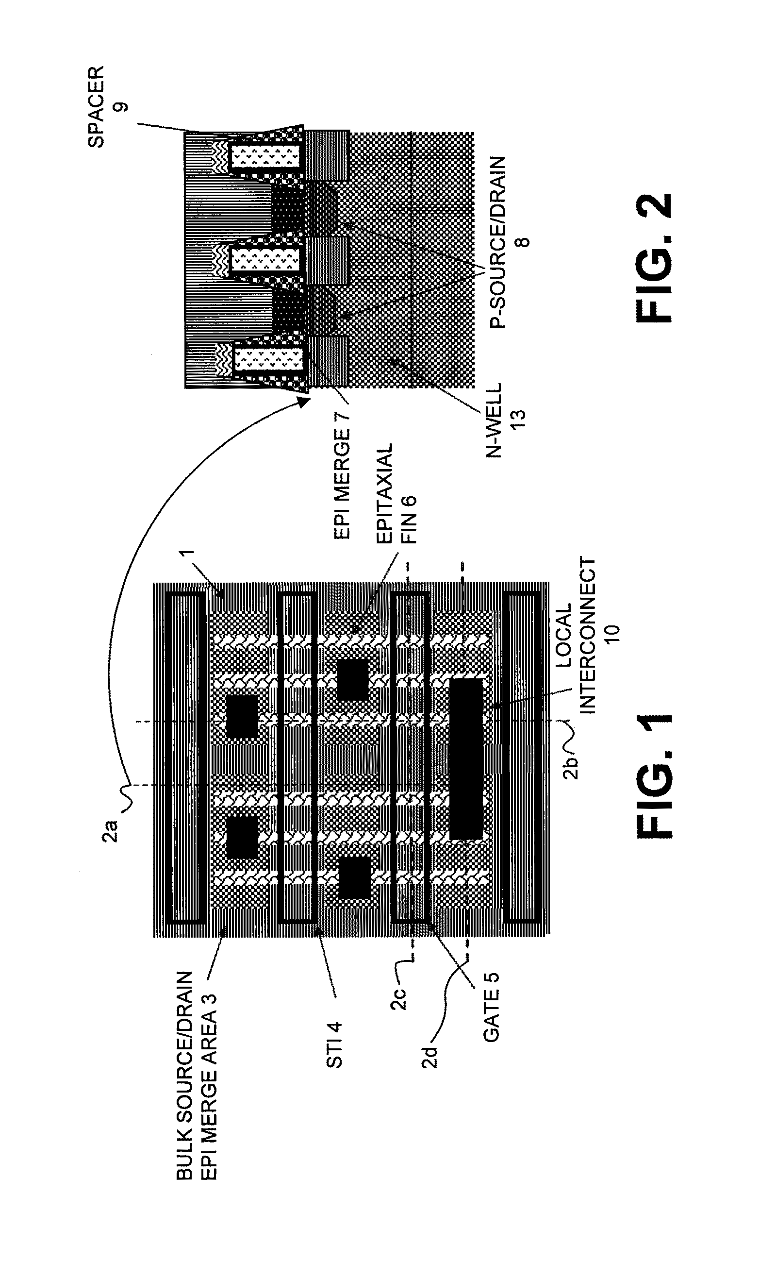
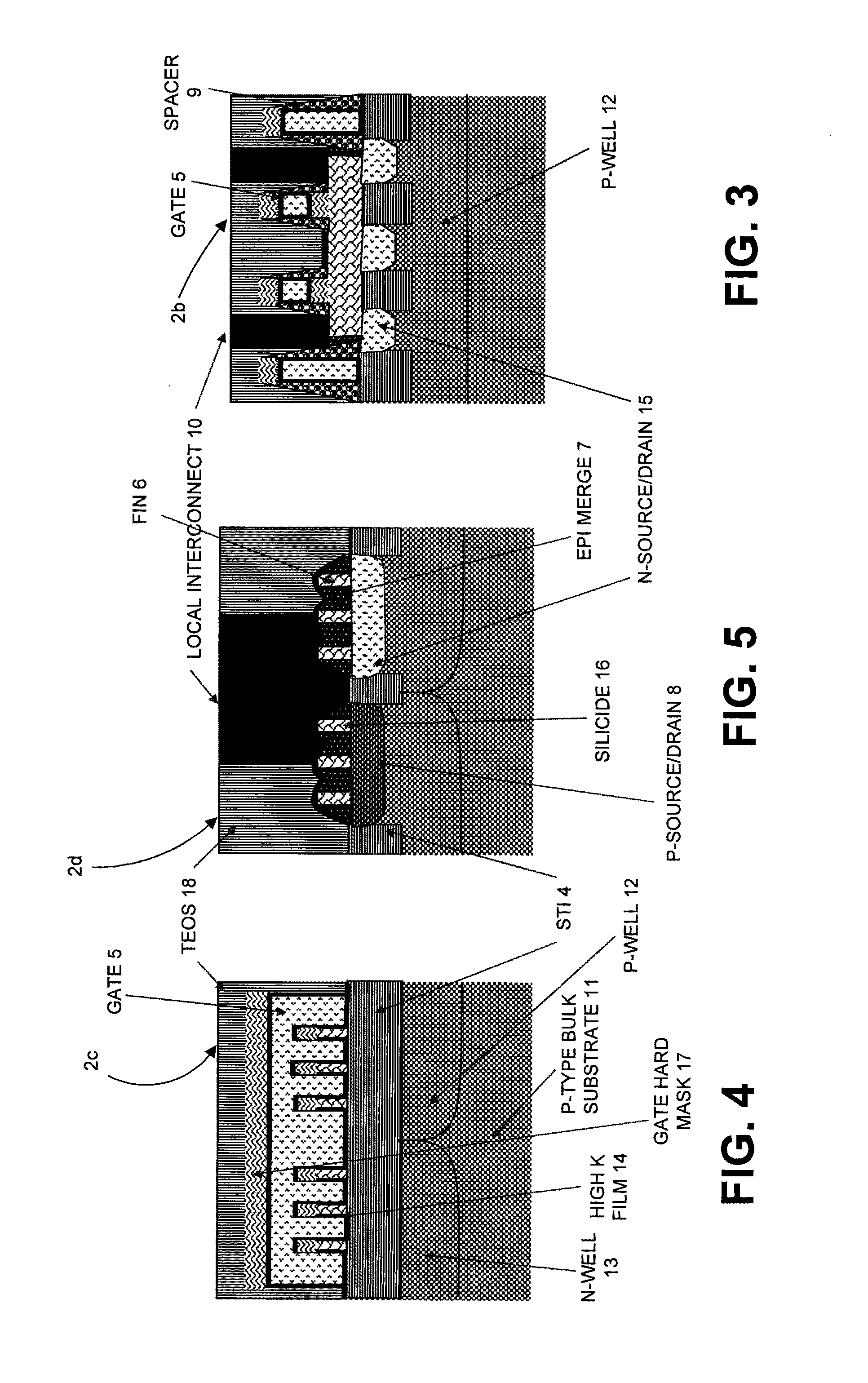
[0040]An integrated fin-based field effect transistor (FinFET) and method of fabricating such devices on a bulk wafer with EPI-defined fin heights over shallow trench isolation (STI) regions are provided. The FinFET channels overlie the STI regions within the semiconductor bulk, while the fins extend beyond the STI regions into the source and drain regions which are implanted within the semiconductor bulk. With bulk source and drain regions, r...


PUM


Abstract

An integrated fin-based field effect transistor (FinFET) and method of fabricating such devices on a bulk wafer with EPI-defined fin heights over shallow trench isolation (STI) regions. The FinFET channels overlie the STI regions within the semiconductor bulk, while the fins extend beyond the STI regions into the source and drain regions which are implanted within the semiconductor bulk. With bulk source and drain regions, reduced external FinFET resistance is provided, and with the fins extending into the bulk source and drain regions, improved thermal properties is provided over conventional silicon on insulator (SOI) devices.

Description

FIELD OF THE DISCLOSURE[0001]The present disclosure relates to multiple gate field effect transistors (FETs), such as metal oxide semiconductor field effect transistors (MOSFETs), and in particular, to Fin-based field effect transistors, also known as FinFETs.BACKGROUND OF THE DISCLOSURE[0002]Perhaps the single most important device in modern electronic systems is the MOSFET. Such devices are used not only as transistors but also as passive devices, such as resistances and capacitances. The ability to scale such devices down to ever smaller dimensions has allowed electronic systems to become smaller to the point of enabling many hand-held and pocket-size systems. However, at the current pace of device scaling, it is predicted that planar transistors will soon reach their limits, in terms of minimize size. Further, as these devices get smaller, they increasingly suffer from undesirable short channel effects, such as off-state leakage current, which increases power consumption by the ...

Claims


Application Information

Patent Timeline
Patent Type & Authority Applications(United States)
IPC IPC(8): H01L29/78H01L21/336
CPCH01L21/845H01L29/785H01L29/66795H01L27/1211
Inventor SCHULTZ, RICHARD T.
Owner ADVANCED MICRO DEVICES INC
Why Eureka
Try Eureka